参数资料
| 型号: | AD8279ARZ-R7 |
| 厂商: | Analog Devices Inc |
| 文件页数: | 8/24页 |
| 文件大小: | 0K |
| 描述: | IC AMP DIFF 1MHZ DUAL LP 14SOIC |
| 标准包装: | 1,000 |
| 放大器类型: | 差分 |
| 电路数: | 2 |
| 输出类型: | 满摆幅 |
| 转换速率: | 1.4 V/µs |
| 增益带宽积: | 1MHz |
| 电压 - 输入偏移: | 50µV |
| 电流 - 电源: | 300µA |
| 电流 - 输出 / 通道: | 15mA |
| 电压 - 电源,单路/双路(±): | 2 V ~ 36 V,±2 V ~ 18 V |
| 工作温度: | -40°C ~ 85°C |
| 安装类型: | 表面贴装 |
| 封装/外壳: | 14-SOIC(0.154",3.90mm 宽) |
| 供应商设备封装: | 14-SOIC |
| 包装: | 带卷 (TR) |
AD8278/AD8279
Rev. C | Page 16 of 24
THEORY OF OPERATION
CIRCUIT INFORMATION
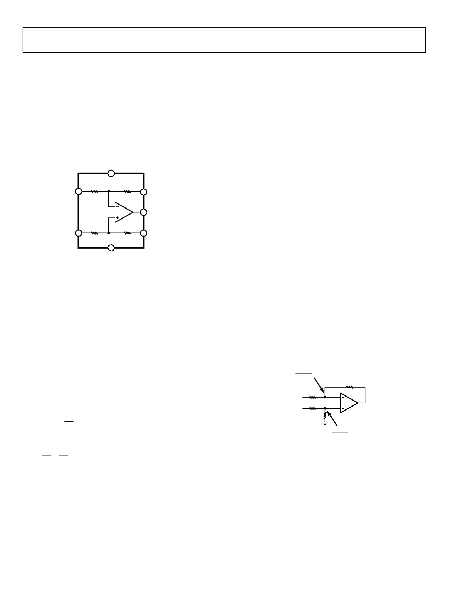
Each channel of the AD8278 and AD8279 consists of a low power,
low noise op amp and four laser-trimmed on-chip resistors.
These resistors can be externally connected to make a variety
of amplifier configurations, including difference, noninverting,
and inverting configurations. Taking advantage of the integrated
resistors of the AD8278 and AD8279 provides the designer with
several benefits over a discrete design, including smaller size,
lower cost, and better ac and dc performance.
2
5
3
1
6
7
4
40k
20k
40k
–VS
+VS
–IN
+IN
SENSE
OUT
REF
20k
AD8278
08
30
8-
0
45
Figure 48. Functional Block Diagram
DC Performance
Much of the dc performance of op amp circuits depends on the
accuracy of the surrounding resistors. Using superposition to
analyze a typical difference amplifier circuit, as is shown in
Figure 49, the output voltage is found to be
+
+
=
+
R3
R4
V
R3
R4
R2
R1
R2
V
IN
OUT
1
This equation demonstrates that the gain accuracy and common-
mode rejection ratio of the AD8278 and AD8279 is determined
primarily by the matching of resistor ratios. Even a 0.1%
mismatch in one resistor degrades the CMRR to 69 dB for a
G = 2 difference amplifier.
The difference amplifier output voltage equation can be reduced to
()
+
=
IN
OUT
V
R3
R4
V
as long as the following ratio of the resistors is tightly matched:
R3
R4
R1
R2 =
The resistors on the AD8278 and AD8279 are laser trimmed to
match accurately. As a result, the AD8278 and AD8279 provide
superior performance over a discrete solution, enabling better
CMRR, gain accuracy, and gain drift, even over a wide tempera-
ture range.
AC Performance
Component sizes and trace lengths are much smaller in an IC
than on a PCB; therefore, the corresponding parasitic elements
are also smaller. This results in better ac performance of the
AD8278 and AD8279. For example, the positive and negative
input terminals of the AD8278 and AD8279 op amps are
intentionally not pinned out. By not connecting these nodes
to the traces on the PCB, their capacitance remains low and
balanced, resulting in improved loop stability and excellent
common-mode rejection over frequency.
DRIVING THE AD8278 AND AD8279
Care should be taken to drive the AD8278 and AD8279 with a
low impedance source, for example, another amplifier. Source
resistance of even a few kilohms (kΩ) can unbalance the resistor
ratios and, therefore, significantly degrade the gain accuracy and
common-mode rejection of the AD8278 and AD8279. Because all
configurations present several kilohms (kΩ) of input resistance,
the AD8278 and AD8279 do not require a high current drive
from the source and are easy to drive.
INPUT VOLTAGE RANGE
The AD8278 and AD8279 are able to measure input voltages
beyond the supply rails. The internal resistors divide down
the voltage before it reaches the internal op amp and provide
protection to the op amp inputs. Figure 49 shows an example
of how the voltage division works in a difference amplifier
configuration. For the AD8278 and AD8279 to measure correctly,
the input voltages at the input nodes of the internal op amp
must stay below 1.5 V of the positive supply rail and can exceed
the negative supply rail by 0.1 V. Refer to the Power Supplies
section for more details.
08
308-062
R4
VIN+
VIN–
R3
R1
R2
R1 + R2
(VIN+)
R2
R1 + R2
(VIN+)
Figure 49. Voltage Division in the Difference Amplifier Configuration
The AD8278 and AD8279 have integrated ESD diodes at the inputs
that provide overvoltage protection. This feature simplifies
system design by eliminating the need for additional external
protection circuitry and enables a more robust system.
The voltages at any of the inputs of the parts can safely range
from +VS 40 V up to VS + 40 V. For example, on ±10 V
supplies, input voltages can go as high as ±30 V. Care should be
taken to not exceed the +VS 40 V to VS + 40 V input limits
to avoid damaging the parts.
相关PDF资料 |
PDF描述 |
|---|---|
| RT0603DRD07110KL | RES 110K OHM 1/10W .5% 0603 SMD |
| AVRL101A1R1NTA | VARISTR 90V 1.1PF STAT PROT 0402 |
| AD8208WBRZ-R7 | IC AMP DIFF PREC 8SOIC |
| AD8277ARZ-R7 | IC AMP GP UNITY GAIN DIFF 14SOIC |
| AVRL101A1R1NTB | VARISTR 39V 1.1PF STAT PROT 0402 |
相关代理商/技术参数 |
参数描述 |
|---|---|
| AD8279ARZ-RL | 功能描述:IC AMP DIFF 1MHZ DUAL LP 14SOIC RoHS:是 类别:集成电路 (IC) >> Linear - Amplifiers - Instrumentation 系列:- 标准包装:50 系列:- 放大器类型:通用 电路数:2 输出类型:满摆幅 转换速率:1.8 V/µs 增益带宽积:6.5MHz -3db带宽:4.5MHz 电流 - 输入偏压:5nA 电压 - 输入偏移:100µV 电流 - 电源:65µA 电流 - 输出 / 通道:35mA 电压 - 电源,单路/双路(±):1.8 V ~ 5.25 V,±0.9 V ~ 2.625 V 工作温度:-40°C ~ 85°C 安装类型:表面贴装 封装/外壳:10-TFSOP,10-MSOP(0.118",3.00mm 宽) 供应商设备封装:10-MSOP 包装:管件 |
| AD8279BRZ | 功能描述:IC AMP DIFF LP 14SOIC RoHS:是 类别:集成电路 (IC) >> Linear - Amplifiers - Instrumentation 系列:- 标准包装:1 系列:- 放大器类型:通用 电路数:4 输出类型:满摆幅 转换速率:0.028 V/µs 增益带宽积:105kHz -3db带宽:- 电流 - 输入偏压:3nA 电压 - 输入偏移:100µV 电流 - 电源:3.3µA 电流 - 输出 / 通道:12mA 电压 - 电源,单路/双路(±):2.7 V ~ 12 V,±1.35 V ~ 6 V 工作温度:-40°C ~ 85°C 安装类型:表面贴装 封装/外壳:14-TSSOP(0.173",4.40mm 宽) 供应商设备封装:14-TSSOP 包装:剪切带 (CT) 其它名称:OP481GRUZ-REELCT |
| AD8279BRZ-R7 | 功能描述:IC AMP DIFF 1MHZ DUAL LP 14SOIC RoHS:是 类别:集成电路 (IC) >> Linear - Amplifiers - Instrumentation 系列:- 标准包装:100 系列:- 放大器类型:通用 电路数:1 输出类型:- 转换速率:0.2 V/µs 增益带宽积:- -3db带宽:- 电流 - 输入偏压:100pA 电压 - 输入偏移:30µV 电流 - 电源:380µA 电流 - 输出 / 通道:- 电压 - 电源,单路/双路(±):±2 V ~ 18 V 工作温度:0°C ~ 70°C 安装类型:表面贴装 封装/外壳:8-SOIC(0.154",3.90mm 宽) 供应商设备封装:8-SO 包装:管件 |
| AD8279BRZ-RL | 功能描述:IC AMP DIFF 1MHZ DUAL LP 14SOIC RoHS:是 类别:集成电路 (IC) >> Linear - Amplifiers - Instrumentation 系列:- 标准包装:100 系列:- 放大器类型:通用 电路数:1 输出类型:- 转换速率:0.2 V/µs 增益带宽积:- -3db带宽:- 电流 - 输入偏压:100pA 电压 - 输入偏移:30µV 电流 - 电源:380µA 电流 - 输出 / 通道:- 电压 - 电源,单路/双路(±):±2 V ~ 18 V 工作温度:0°C ~ 70°C 安装类型:表面贴装 封装/外壳:8-SOIC(0.154",3.90mm 宽) 供应商设备封装:8-SO 包装:管件 |
| AD8279-EVALZ | 功能描述:AD8279 2 - Dual Channels per IC Difference Amplifier Evaluation Board 制造商:analog devices inc. 系列:- 零件状态:有效 每 IC 通道数:2 - 双 放大器类型:差异 输出类型:单端,满摆幅 压摆率:1.4 V/μs -3db 带宽:1MHz 电流 - 输出/通道:15mA 工作温度:-40°C ~ 85°C 电流 - 电源(主 IC):300μA 电压 - 电源,单/双(±):2 V ~ 36 V,±2 V ~ 18 V 板类型:完全填充 所含物品:板 使用的 IC/零件:AD8279 标准包装:1 |
发布紧急采购,3分钟左右您将得到回复。