参数资料
| 型号: | AD8307AR-REEL |
| 厂商: | Analog Devices Inc |
| 文件页数: | 7/24页 |
| 文件大小: | 0K |
| 描述: | IC LOGARITHMIC AMP 8-SOIC T/R |
| 标准包装: | 2,500 |
| 类型: | 对数放大器 |
| 应用: | 接收器信号强度指示(RSSI) |
| 安装类型: | 表面贴装 |
| 封装/外壳: | 8-SOIC(0.154",3.90mm 宽) |
| 供应商设备封装: | 8-SO |
| 包装: | 带卷 (TR) |
AD8307
Rev. D | Page 15 of 24
In most applications, the signal is single sided and can be applied
to either Pin 1 or Pin 8, with the other pin ac-coupled to ground.
Under these conditions, the largest input signal that can be
handled by the AD8307 is 10 dBm (sine amplitude of ±1 V)
when operating from a 3 V supply; 16 dBm can be handled
using a 5 V supply. The full 16 dBm can be achieved for supplies
down to 2.7 V, using a fully balanced drive. For frequencies
above about 10 MHz, this is most easily achieved using a matching
network. Using such a network, having an inductor at the input,
the input transient is eliminated. Occasionally, it is desirable to
use the dc-coupled potential of the AD8307. The main challenge
is to present signals to the log amp at the elevated common-mode
input level, requiring the use of low noise, low offset buffer
amplifiers. Using dual supplies of ±3 V, the input pins can
operate at ground potential.
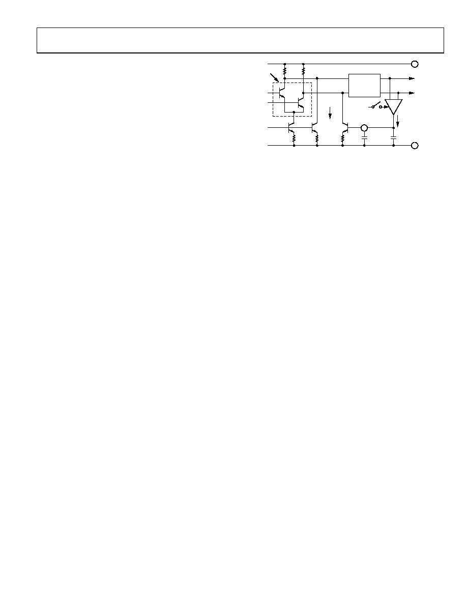
OFFSET INTERFACE
The input-referred dc offsets in the signal path are nulled via
the interface associated with Pin 3, shown in Figure 30. Q1 and
Q2 are the first stage input transistors, with their corresponding
load resistors (125 Ω). Q3 and Q4 generate small currents, which
can introduce a dc offset into the signal path. When the voltage
on OFS is at about 1.5 V, these currents are equal and nominally
64 μA. When OFS is taken to ground, Q4 is off and the effect of the
current in Q3 is to generate an offset voltage of 64 μV × 125 Ω =
8 mV. Because the first stage gain is ×5, this is equivalent to an
input offset (INP to INM) of 1.6 mV. When OFS is taken to its
most positive value, the input-referred offset is reversed to 1.6 mV.
If true dc coupling is needed, down to very small inputs, this auto-
matic loop must be disabled and the residual offset eliminated
using a manual adjustment.
In normal operation, however, using an ac-coupled input signal,
the OFS pin should be left open. Any residual input offset voltage
is then automatically nulled by the action of the feedback loop.
The gm cell, which is gated off when the chip is disabled, converts
any output offset (sensed at a point near the end of the cascade
of amplifiers) to a current. This is integrated by the on-chip
capacitor, CHP, and any added external capacitance, COFS, to
generate an error voltage, which is applied back to the input
stage in the polarity needed to null the output offset. From a
small signal perspective, this feedback alters the response of the
amplifier, which, rather than behaving as a fully dc-coupled
system, now exhibits a zero in its ac transfer function, resulting
in a closed-loop high-pass corner at about 1.5 MHz.
48k
125
MAIN GAIN
STAGES
Q2
Q1
Q3
64A AT
BALANCE
Q4
S
AVERAGE
ERROR
CURRENT
OFS
TO LAST
DETECTOR
COFS
CHP
COM
VPS
36k
INPUT
STAGE
01082-
030
BIAS, ~1.2V
2
3
7
gm
Figure 30. Offset Interface and Offset Nulling Path
The offset feedback is limited to a range of ±1.6 mV; signals larger
than this override the offset control loop, which only affects perfor-
mance for very small inputs. An external capacitor reduces the
high-pass corner to arbitrarily low frequencies; using 1 μF, this
corner is below 10 Hz. All Analog Devices log amps use an offset
nulling loop; the AD8307 differs in using this single-sided form.
OUTPUT INTERFACE
The outputs from the nine detectors are differential currents,
having an average value that is dependent on the signal input
level, plus a fluctuation at twice the input frequency. The currents
are summed at Node LGP and Node LGM in Figure 31. Further
currents are added at these nodes, to position the intercept, by
slightly raising the output for zero input, and to provide tempera-
ture compensation. Because the AD8307 is not laser trimmed,
there is a small uncertainty in both the log slope and the log
intercept. These scaling parameters can be adjusted.
For zero signal conditions, all the detector output currents are
equal. For a finite input of either polarity, their difference is
converted by the output interface to a single-sided unipolar
current nominally scaled 2 μA/dB (40 μA/decade) at Pin OUT.
An on-chip 12.5 kΩ resistor, R1, converts this current to a voltage
of 25 mV/dB. C1 and C2 are effectively in shunt with R1 and form
a low-pass filter pole with a corner frequency of about 5 MHz.
The pulse response settles to within 1% of the final value within
300 ns. This integral low-pass filter provides adequate smoothing
in many IF applications. At 10.7 MHz, the 2f ripple is 12.5 mV
in amplitude, equivalent to ±0.5 dB, and only 0.5 mV (±0.02 dB)
at f = 50 MHz. A filter capacitor, CFLT, added from Pin OUT to
ground lowers this corner frequency. Using 1 μF, the ripple is
maintained to less than ±0.5 dB down to input frequencies of
100 Hz. Note that COFS should also be increased in low frequency
applications, and is typically made equal to CFLT.
相关PDF资料 |
PDF描述 |
|---|---|
| AD7243AR | IC SRL DAC 12BIT LC2MOS 16-SOIC |
| ADA4960-1ACPZ-RL | IC ADC DRIVER DIFF 16LFCSP |
| VE-25N-IV-F3 | CONVERTER MOD DC/DC 18.5V 150W |
| LTC6405CMS8E#PBF | IC AMP/DRVR DIFF R-R 5V 8-MSOP |
| SY88843VMG | IC AMP LIMIT CML TTL SD 16MLF |
相关代理商/技术参数 |
参数描述 |
|---|---|
| AD8307AR-REEL7 | 功能描述:IC LOGARITHMIC AMP 8-SOIC RoHS:否 类别:集成电路 (IC) >> 线性 - 放大器 - 专用 系列:- 产品培训模块:Lead (SnPb) Finish for COTS Obsolescence Mitigation Program 标准包装:60 系列:- 类型:可变增益放大器 应用:CATV 安装类型:表面贴装 封装/外壳:20-WQFN 裸露焊盘 供应商设备封装:20-TQFN-EP(5x5) 包装:托盘 |
| AD8307ARZ | 功能描述:IC LOGARITHMIC AMP 92DB 8-SOIC RoHS:是 类别:集成电路 (IC) >> 线性 - 放大器 - 专用 系列:- 产品培训模块:Lead (SnPb) Finish for COTS Obsolescence Mitigation Program 标准包装:60 系列:- 类型:可变增益放大器 应用:CATV 安装类型:表面贴装 封装/外壳:20-WQFN 裸露焊盘 供应商设备封装:20-TQFN-EP(5x5) 包装:托盘 |
| AD8307ARZ | 制造商:Analog Devices 功能描述:Logarithmic Amplifier IC |
| AD8307ARZ-REEL | 功能描述:IC AMP LOGARITHMIC 8SOIC RoHS:是 类别:集成电路 (IC) >> 线性 - 放大器 - 专用 系列:- 产品培训模块:Lead (SnPb) Finish for COTS Obsolescence Mitigation Program 标准包装:60 系列:- 类型:可变增益放大器 应用:CATV 安装类型:表面贴装 封装/外壳:20-WQFN 裸露焊盘 供应商设备封装:20-TQFN-EP(5x5) 包装:托盘 |
| AD8307ARZ-RL7 | 功能描述:IC AMP LOGARITHMIC 8-SOIC RoHS:是 类别:集成电路 (IC) >> 线性 - 放大器 - 专用 系列:- 产品培训模块:Lead (SnPb) Finish for COTS Obsolescence Mitigation Program 标准包装:60 系列:- 类型:可变增益放大器 应用:CATV 安装类型:表面贴装 封装/外壳:20-WQFN 裸露焊盘 供应商设备封装:20-TQFN-EP(5x5) 包装:托盘 |
发布紧急采购,3分钟左右您将得到回复。