参数资料
| 型号: | AD830AR |
| 厂商: | Analog Devices Inc |
| 文件页数: | 4/20页 |
| 文件大小: | 0K |
| 描述: | IC VIDEO DIFF AMP HS 8-SOIC |
| 标准包装: | 98 |
| 应用: | 差分 |
| 电路数: | 1 |
| -3db带宽: | 85MHz |
| 转换速率: | 360 V/µs |
| 电流 - 电源: | 14.5mA |
| 电流 - 输出 / 通道: | 50mA |
| 电压 - 电源,单路/双路(±): | 8 V ~ 33 V,±4 V ~ 16.5 V |
| 安装类型: | 表面贴装 |
| 封装/外壳: | 8-SOIC(0.154",3.90mm 宽) |
| 供应商设备封装: | 8-SOIC |
| 包装: | 管件 |
AD830
Rev. C | Page 12 of 20
VX1
VOUT
IY
IX
CC
A = 1
GM
AOLS=
GMRP
VX2
GM
VY1
VY2
RP
IZ
IX = (VX1 – VX2) GM
IY = (VY1 – VY2) GM
IZ = IX + IY
1 + S (CCRP)
0
08
81
-02
6
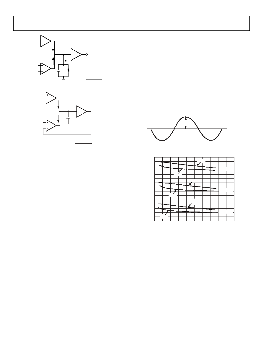
Figure 26. Topology Diagram
VX1
VOUT
IY
IX
CC
A = 1
GM
1
VX2
GM
VY1
VY2
VX1 – VX2 = VY2 – VY1
FOR VY2 = VOUT
VOUT = (VX1 – VX2 + VY1)
1 + S(CC/GM)
00
88
1-
02
7
Figure 27. Closed-Loop Connection
Precise amplification is accomplished through closed-loop
operation of this topology. Voltage feedback is implemented via
the Y GM stage where the output is connected to the Y input
for negative feedback, as shown in Figure 27. An input signal is
applied across the X GM stage, either fully differential or single-
ended referred to common. It produces a current signal that is
summed at the high impedance node with the output current
from the Y GM stage. Negative feedback nulls this sum to a small
error current necessary to develop the output voltage at the high
impedance node. The error current is usually negligible, so the
null condition essentially forces the Y GM output stage current
to equal the exact X GM output current. Because the two
transconductances are identical, the differential voltage across
the Y inputs equals the negative of the differential voltage across
the X input; VY = VX or, more precisely, VY2 VY1 = VX1 VX2.
This simple relation provides the basis to easily analyze any
function possible to synthesize with the AD830, including any
feedback situation.
The bandwidth of the circuit is defined by the GM and the
capacitor, CC. The highly linear GM stages give the amplifier a
single-pole response, excluding the output amplifier and
loading effects. It is important to note that the bandwidth and
general dynamic behavior is symmetrical (identical) for the
noninverting and the inverting connections of the AD830. In
addition, the input impedance and CMRR are the same for
either connection. This is very advantageous and unlike in a
voltage or current feedback amplifier where there is a distinct
difference in performance between the inverting and
noninverting gain. The practical importance of this cannot be
overemphasized and is a key feature offered by the AD830
amplifier topology.
INTERFACING THE INPUT
Common-Mode Voltage Range
The common-mode range of the AD830 is defined by the
amplitude of the differential input signal and the supply voltage.
The general definition of common-mode voltage, VCM, is
usually applied to a symmetrical differential signal centered
around a particular voltage, as illustrated in Figure 28. This is
the meaning implied here for common-mode voltage. The
internal circuitry establishes the maximum allowable voltage on
the input or feedback pins for a given supply voltage. This
constraint and the differential input voltage sets the common-
mode voltage limit. Figure 29 shows a curve of the common-
mode voltage range versus the differential voltage for three
supply voltage settings.
VMAX
VCM
VPEAK
00
88
1-
02
8
Figure 28. Common-Mode Definition
DIFFERENTIAL INPUT VOLTAGE (VPEAK)
15
0
CO
M
O
N-
M
O
DE
V
O
L
T
2.0
A
GE
(
±
V
)
0.4
0.8
1.2
1.6
6
3
12
9
±5V = VS
±15V = VS
–VCM
+VCM
±10V = VS
–VCM
00
88
1-
02
9
Figure 29. Input Common-Mode Voltage Range vs. Differential Input Voltage
Differential Voltage Range
The maximum applied differential voltage is limited by the
clipping range of the input stages. This is nominally set at a
2.4 V magnitude and depicted in the cross plot (X-Y) in Figure 30.
The useful linear range of the input stages is set at 2 V but is
actually a function of the distortion required for a particular
application. The distortion increases for larger differential input
voltages. A plot of relative distortion versus the input differential
characteristics impose a secondary limit to the differential input
voltage for high accuracy applications.
相关PDF资料 |
PDF描述 |
|---|---|
| VI-J4B-MZ-B1 | CONVERTER MOD DC/DC 95V 25W |
| 6-1877846-6 | PLUG 6POS 80 DEG BLK/BLU 2.7-3.9 |
| AD811AN | IC CURR-FDBK AMP VIDEO HS 8-DIP |
| 6-1877846-0 | PLUG 6POS 80 DEG GRY/GRN 2.7-3.9 |
| 5-1877846-4 | PLUG 6POS 80 DEG BLK/GRN 2.7-3.9 |
相关代理商/技术参数 |
参数描述 |
|---|---|
| AD830AR-REEL | 制造商:Analog Devices 功能描述:Video Amp Single 85MHz |
| AD830ARREEL7 | 制造商:AD 功能描述:* |
| AD830AR-REEL7 | 制造商:Analog Devices 功能描述:Video Amp Single 85MHz |
| AD830ARZ | 功能描述:IC VIDEO DIFF AMP HS 8-SOIC RoHS:是 类别:集成电路 (IC) >> 线性 - 放大器 - 视频放大器和频缓冲器 系列:- 产品培训模块:Lead (SnPb) Finish for COTS Obsolescence Mitigation Program 标准包装:50 系列:- 应用:TFT-LCD 面板:VCOM 驱动器 输出类型:满摆幅 电路数:1 -3db带宽:35MHz 转换速率:40 V/µs 电流 - 电源:3.7mA 电流 - 输出 / 通道:1.3A 电压 - 电源,单路/双路(±):9 V ~ 20 V,±4.5 V ~ 10 V 安装类型:表面贴装 封装/外壳:8-TSSOP,8-MSOP(0.118",3.00mm 宽)裸露焊盘 供应商设备封装:8-uMax-EP 包装:管件 |
| AD830ARZ | 制造商:Analog Devices 功能描述:IC, VIDEO DIFF AMP, DUAL, 85MHZ, SOIC-8 |
发布紧急采购,3分钟左右您将得到回复。