参数资料
| 型号: | AD830JRZ-R7 |
| 厂商: | Analog Devices Inc |
| 文件页数: | 5/20页 |
| 文件大小: | 0K |
| 描述: | IC VIDEO DIFF AMP HS 8-SOIC T/R |
| 标准包装: | 1 |
| 应用: | 差分 |
| 电路数: | 1 |
| -3db带宽: | 85MHz |
| 转换速率: | 360 V/µs |
| 电流 - 电源: | 14.5mA |
| 电流 - 输出 / 通道: | 50mA |
| 电压 - 电源,单路/双路(±): | 8 V ~ 33 V,±4 V ~ 16.5 V |
| 安装类型: | 表面贴装 |
| 封装/外壳: | 8-SOIC(0.154",3.90mm 宽) |
| 供应商设备封装: | 8-SOIC |
| 包装: | 标准包装 |
| 产品目录页面: | 764 (CN2011-ZH PDF) |
| 其它名称: | AD830JRZ-R7DKR |
AD830
Rev. C | Page 13 of 20
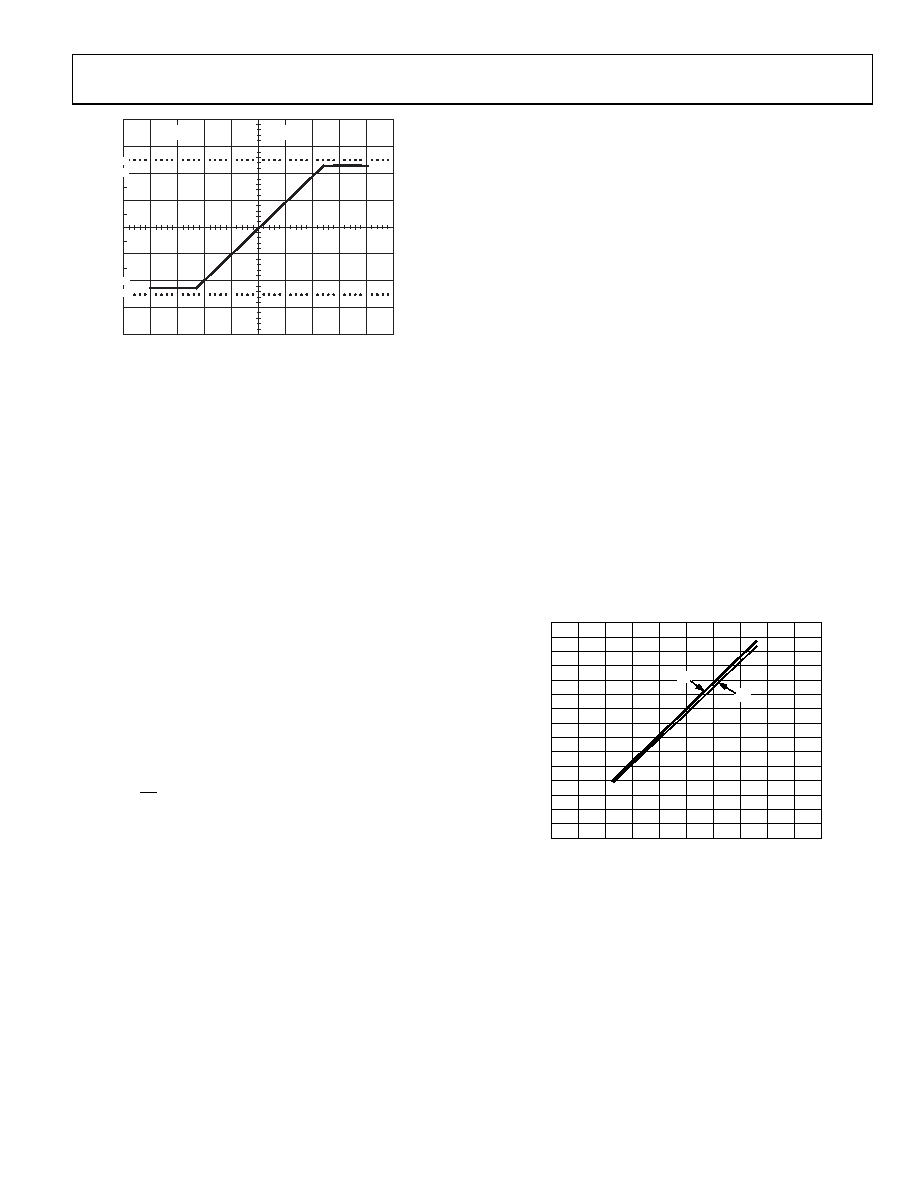
10
0%
100
90
1V
00
88
1-
0
30
Figure 30. Clipping Behavior
Choice of Polarity
The sign of the gain is easily selected by choosing the polarity
of the connections to the + and inputs of the X GM stage.
Swapping between inverting and noninverting gain is possible
simply by reversing the input connections. The response of the
amplifier is identical in either connection, except for the sign
change.
The bandwidth, high impedance, and transient behavior of the
AD830 is symmetrical for both polarities of gain. This is very
advantageous and unlike an op amp.
Input Impedance
The relatively high input impedance of the AD830, for a
differential receiver amplifier, permits connections to modest
impedance sources without much loading or loss of common-
mode rejection. The nominal input resistance is 300 kΩ. The
real limit to the upper value of the source resistance is in its
effect on common-mode rejection and bandwidth. If the source
resistance is in only one input, then the low frequency
common-mode rejection is lowered to ≈ RIN/RS. The source
resistance/input capacitance pole limits the bandwidth. Refer to
the following equation:
×
π
=
IN
S
C
R
f
2
1
Furthermore, the high frequency common-mode rejection is
additionally lowered by the difference in the frequency response
caused by the RS × CIN pole. Therefore, to maintain good low
and high frequency common-mode rejection, it is recommended
that the source resistances of the + and inputs be matched and
of modest value (≤10 kΩ).
Handling Bias Currents
The bias currents are typically 4 μA flowing into each pin of the
GM stages of the AD830. Because all applications possess some
finite source resistance, the bias current through this resistor
creates a voltage drop (IBIAS × RS). The relatively high input
impedance of the AD830 permits modest values of RS, typically
≤10 kΩ. If the source resistance is in only one terminal, then an
objectionable offset voltage may result, for example, 4 μA × 5
kΩ = 20 mV. Placement of an equal value resistor in series with
mismatches in the resistances, a residual offset remains and is
likely to be greater than the bias current (offset current)
mismatches.
Applying Fee
the other input cancels the offset to first order. However, due to
dback
for use with gains from 1 to 100. Gains
hat
y
830 is defined by the differential
n
ge
e
The AD830 is intended
greater than one are simply set by a pair of resistors connected
as shown in the difference amplifier (Figure 40) with gain >1.
The value of the bottom resistor, R2, should be kept less than
1 kΩ to ensure that the pole formed by CIN and the parallel
connection of R1 and R2 is sufficiently high in frequency so t
it does not introduce excessive phase shift around the loop and
destabilize the amplifier. A compensating resistor, equal to the
parallel combination of R1 and R2, should be placed in series
with the other Y GM stage input to preserve the high frequenc
common-mode rejection and to lower the offset voltage
induced by the input bias current.
Output Common Mode
The output swing of the AD
input voltage, the gain, and the output common. Depending o
the anticipated signal span, the output common (or ground)
may be set anywhere between the allowable peak output volta
in a manner similar to that described for input voltage common
mode. A plot of the peak output voltage versus the supply is
shown in Figure 31. A prediction of the common-mode rang
versus the peak output differential voltage can be easily derived
from the maximum output swing as VOCM = VMAX VPEAK.
SUPPLY VOLTAGE (V)
15
0
20
0
MA
X
IMU
M
O
U
T
P
U
T
S
W
IN
G
(±
V
)
48
12
16
6
3
12
9
VP
VN
00
88
1-
0
31
Figure 31. Maximum Output Swing vs. Supply
Output Cur
output current is set by the short-circuit
nto
rent
The absolute peak
current limiting, typically greater than 60 mA. The maximum
drive capability is rated at 50 mA but without a guarantee of
distortion performance. Best distortion performance is obtained
by keeping the output current ≤20 mA. Attempting to drive
large voltages into low valued resistances, for example, 10 V i
150 Ω causes an apparent lowering of the limit for output signal
swing but is just the current limiting behavior.
相关PDF资料 |
PDF描述 |
|---|---|
| LTC1597BIG | IC D/A CONV 16BIT PAR 28-SSOP |
| LTC1597-1BIG#PBF | IC D/A CONV 16BIT PAR 28-SSOP |
| VI-BN0-MU | CONVERTER MOD DC/DC 5V 200W |
| VI-BN2-MU | CONVERTER MOD DC/DC 15V 200W |
| VE-23J-IV-F2 | CONVERTER MOD DC/DC 36V 150W |
相关代理商/技术参数 |
参数描述 |
|---|---|
| AD830JRZ-RL | 功能描述:IC VIDEO DIFF AMP HS 8-SOIC T/R RoHS:是 类别:集成电路 (IC) >> 线性 - 放大器 - 视频放大器和频缓冲器 系列:- 标准包装:1,000 系列:- 应用:驱动器 输出类型:差分 电路数:3 -3db带宽:350MHz 转换速率:1000 V/µs 电流 - 电源:14.5mA 电流 - 输出 / 通道:60mA 电压 - 电源,单路/双路(±):5 V ~ 12 V,±2.5 V ~ 6 V 安装类型:表面贴装 封装/外壳:20-VFQFN 裸露焊盘 供应商设备封装:20-QFN 裸露焊盘(4x4) 包装:带卷 (TR) |
| AD830SQ/883B | 制造商:未知厂家 制造商全称:未知厂家 功能描述:Single Video Amplifier |
| AD831 | 制造商:AD 制造商全称:Analog Devices 功能描述:Low Distortion Mixer |
| AD8310 | 制造商:AD 制造商全称:Analog Devices 功能描述:Fast, Voltage-Out DC-440 MHz 95 dB Logarithmic Amplifier |
| AD8310_05 | 制造商:AD 制造商全称:Analog Devices 功能描述:Fast, Voltage-Out DC-440 MHz, 95 dB Logarithmic Amplifier |
发布紧急采购,3分钟左右您将得到回复。