- 您现在的位置:买卖IC网 > PDF目录10602 > AD8324ACPZ-REEL7 (Analog Devices Inc)IC LINE DRIVER CATV 3.3V 20LFCSP PDF资料下载
参数资料
| 型号: | AD8324ACPZ-REEL7 |
| 厂商: | Analog Devices Inc |
| 文件页数: | 14/16页 |
| 文件大小: | 0K |
| 描述: | IC LINE DRIVER CATV 3.3V 20LFCSP |
| 标准包装: | 1,500 |
| 类型: | 线路驱动器,发射器 |
| 应用: | 调制解调器,CATV |
| 安装类型: | 表面贴装 |
| 封装/外壳: | 20-VFQFN 裸露焊盘,CSP |
| 供应商设备封装: | 20-LFCSP-VQ |
| 包装: | 带卷 (TR) |
Data Sheet
AD8324
Rev. B | Page 7 of 16
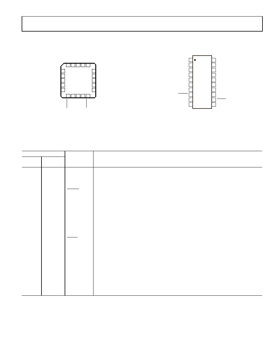
PIN CONFIGURATIONS AND FUNCTION DESCRIPTIONS
Figure 5. 20-Lead LFCSP Pin Configuration
Figure 6. 20-Lead QSOP Pin Configuration
Table 6. Pin Function Descriptions
Pin No.
20-Lead
LFCSP
20-Lead
QSOP
Mnemonic
Description
1, 2, 5, 9,
18, 19
1, 3, 4, 7,
11, 20
GND
Common External Ground Reference.
3
5
VIN+
Noninverting Input. DC-biased to approximately VCC/2. Must be ac-coupled with a 0.1 μF capacitor.
4
6
VIN–
Inverting Input. DC-biased to approximately VCC/2. Must be ac-coupled with a 0.1 μF capacitor.
6
8
DATEN
Data Enable Low Input. This port controls the 8-bit parallel data latch and shift register. A Logic 0
to Logic 1 transition transfers the latched data to the attenuator core (updates the gain) and
simultaneously inhibits serial data transfer into the register. A Logic 1 to Logic 0 transition inhibits
the data latch (holds the previous and simultaneously enables the register for serial data load).
7
9
SDATA
Serial Data Input. This digital input allows an 8-bit serial (gain) word to be loaded into the internal
register with the most significant bit (MSB) first.
8
10
CLK
Clock Input. The clock port controls the serial attenuator data transfer rate to the 8-bit master-
slave shift register. Logic 0 to Logic 1 transition latches the data bit, and a Logic 1 to Logic 0
transfers the data bit to the slave. This requires the input serial data-word to be valid at or before
this clock transition.
10
12
SLEEP
Low Power Sleep Mode. In sleep mode, the supply current of the AD8324 is reduced to 30 μA. A
Logic 0 powers down the part (high ZOUT state), and a Logic 1 powers up the part.
11
13
NC
No Connect. Do not connect to this pin.
12
14
BYP
Internal Bypass. This pin must be externally decoupled (0.1 μF capacitor).
13
15
VOUT–
14
16
VOUT+
15
17
RAMP
External RAMP Capacitor (Optional).
16
18
TXEN
Transmit Enable. Logic 0 disables forward transmission, and Logic 1 enables forward transmission.
17, 20
2, 19
VCC
Common Positive External Supply Voltage.
0
Not
applicable
EPAD
Exposed Pad. The exposed pad must be connected to a solid copper plane with low thermal
resistance. This applies to the 20-lead LFCSP package only.
TOP VIEW
(Not to Scale)
AD8324
1
2
3
4
5
15
14
13
12
11
16
17
20 19 18
67
8
9
10
GND
NOTES
1. NC = NO CONNECT. DO NOT CONNECT TO THIS PIN.
2. THE EXPOSED PAD MUST BE CONNECTED TO A SOLID COPPER PLANE
WITH A LOW THERMAL RESISTANCE. THIS APPLIES TO THE 20-LEAD
LFCSP PACKAGE ONLY.
VIN+
VIN–
GN
D
GN
D
V
CC
V
CC
TX
EN
GN
D
SL
E
EP
DA
T
E
N
SDA
T
A
CL
K
RAMP
VOUT+
VOUT–
BYP
NC
0
433
9-
0
-00
6
TOP VIEW
(Not to Scale)
20
19
18
17
16
15
14
13
12
11
1
2
3
4
5
6
7
8
9
10
AD8324
TXEN
SDATA
VCC
CLK
VIN+
SLEEP
BYP
NC
VOUT+
NC = NO CONNECT
GND
VIN–
GND
RAMP
VOUT–
GND
VCC
DATEN
04339-0-005
相关PDF资料 |
PDF描述 |
|---|---|
| HR25-9R-16P | CONN RECEPT 16POS MALE PANEL MT |
| VE-BWJ-IV-F3 | CONVERTER MOD DC/DC 36V 150W |
| UPC3228T5S-E2-A | IC DOWNCONVERTER LD 32-QFN |
| MAX1480ECCPI+ | IC RS485/RS422 DATA INTRFC 28DIP |
| MAX1490EBCPG+ | IC RS485/RS422 DATA INTRFC 24DIP |
相关代理商/技术参数 |
参数描述 |
|---|---|
| AD8324JRQ | 制造商:Analog Devices 功能描述:SP Amp Line Driver Amp Single 3.47V 20-Pin QSOP Tube 制造商:Rochester Electronics LLC 功能描述:LOW COST 3.3V CABLE LINE DRIVER - Bulk 制造商:Analog Devices 功能描述:CABLE LINE DRIVER 3.3V SMD 8324 |
| AD8324JRQ-EVAL | 制造商:AD 制造商全称:Analog Devices 功能描述:3.3 V Upstream Cable Line Driver |
| AD8324JRQ-REEL | 制造商:Analog Devices 功能描述:SP Amp Line Driver Amp Single 3.47V 20-Pin QSOP T/R 制造商:Analog Devices 功能描述:SP AMP LINE DRVR AMP SGL 3.47V 20QSOP - Tape and Reel |
| AD8324JRQ-REEL7 | 制造商:Analog Devices 功能描述:SP Amp Line Driver Amp Single 3.47V 20-Pin QSOP T/R 制造商:Analog Devices 功能描述:SP AMP LINE DRVR AMP SGL 3.47V 20QSOP - Tape and Reel |
| AD8324JRQZ | 制造商:Analog Devices 功能描述:SP Amp Line Driver Amp Single 3.47V 20-Pin QSOP Tube |
发布紧急采购,3分钟左右您将得到回复。