- 您现在的位置:买卖IC网 > PDF目录10616 > AD8325ARUZ (Analog Devices Inc)IC LN DVR CATV FINE-STEP 28TSSOP PDF资料下载
参数资料
| 型号: | AD8325ARUZ |
| 厂商: | Analog Devices Inc |
| 文件页数: | 1/16页 |
| 文件大小: | 0K |
| 描述: | IC LN DVR CATV FINE-STEP 28TSSOP |
| 标准包装: | 50 |
| 类型: | 线路驱动器,发射器 |
| 应用: | 调制解调器,机顶盒 |
| 安装类型: | 表面贴装 |
| 封装/外壳: | 28-TSSOP(0.173",4.40mm 宽) |
| 供应商设备封装: | 28-TSSOP |
| 包装: | 管件 |
a
5 V CATV Line Driver Fine Step
Output Power Control
AD8325
FEATURES
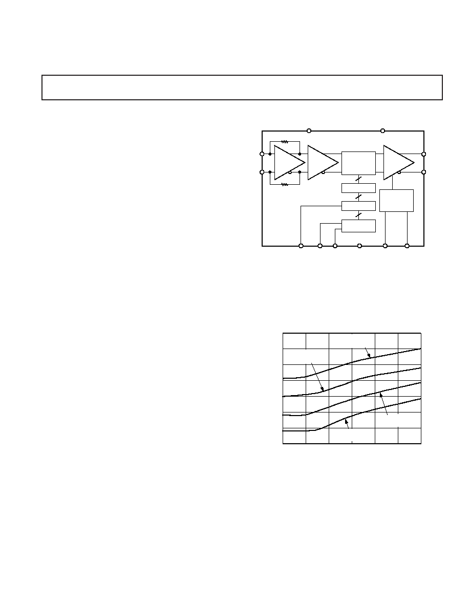
FUNCTIONAL BLOCK DIAGRAM
Supports DOCSIS Standard for Reverse Path
VCC (7 PINS)
BYP
Transmission
Gain Programmable in 0.75 dB Steps Over a 59.45 dB
Range
Low Distortion at 61 dBmV Output
VIN+
–57 dBc SFDR at 21 MHz
DIFF OR
SINGLE
INPUT
AMP
ATTENUATION
CORE
ZOUT DIFF =
75
8
ZIN (SINGLE) = 800
ZIN (DIFF) = 1.6k
R1
R2
AD8325
VERNIER
DECODE
DATA LATCH
SHIFT
REGISTER
POWER-DOWN
LOGIC
POWER
AMP
Output Noise Level
–48 dBmV in 160 kHz
Maintains 75
Output Impedance
Transmit Enable and Transmit Disable Modes
Upper Bandwidth: 100 MHz (Full Gain Range)
5 V Supply Operation
Supports SPI Interfaces
APPLICATIONS
Gain-Programmable Line Driver
–55 dBc SFDR at 42 MHz
VIN–
VOUT+
VOUT–
DOCSIS High-Speed Data Modems
Interactive Cable Set-Top Boxes
PC Plug-in Cable Modems
General-Purpose Digitally Controlled Variable Gain Block
GENERAL DESCRIPTION
The AD8325 is a low-cost, digitally controlled, variable gain ampli
fier optimized for coaxial line driving applications such as cable
modems that are designed to the MCNS-DOCSIS upstream
–50
standard. An 8-bit serial word determines the desired output gain
over a 59.45 dB range resulting in gain changes of 0.7526 dB/LSB.
–52
The AD8325 comprises a digitally controlled variable attenuator
–54
of 0 dB to –59.45 dB, which is preceded by a low noise, fixed
gain buffer and is followed by a low distortion high power ampli
fier. The AD8325 accepts a differential or single-ended input
signal. The output is specified for driving a 75
W load, such as
coaxial cable.
DISTORTION
–
dBc
–56
–58
Distortion performance of –57 dBc is achieved with an output
–60
level up to 61 dBmV at 21 MHz bandwidth. A key performance
–62
and cost advantage of the AD8325 results from the ability to
maintain a constant 75
W output impedance during Transmit
–64
DATEN
DATACLK
GND (11 PINS)
TXEN
SLEEP
VOUT
VOUT = 62dBmV
@ MAX GAIN
= 61dBmV
@ MAX GAIN
VOUT = 60dBmV
@ MAX GAIN
VOUT = 59dBmV
@ MAX GAIN
Enable and Transmit Disable conditions. In addition, this
5
15
25
35
45
55
device has a sleep mode function that reduces the quiescent
FUNDAMENTAL FREQUENCY – MHz
current to 4 mA.
Figure 1. Worst Harmonic Distortion vs. Gain Control
The AD8325 is packaged in a low-cost 28-lead TSSOP, operates
from a single 5 V supply, and has an operational temperature
range of –40
∞C to +85∞C.
REV. A
Information furnished by Analog Devices is believed to be accurate and
reliable. However, no responsibility is assumed by Analog Devices for its
use, nor for any infringements of patents or other rights of third parties that
may result from its use. No license is granted by implication or otherwise
One Technology Way, P.O. Box 9106, Norwood, MA 02062-9106, U.S.A.
under any patent or patent rights of Analog Devices. Trademarks and
Tel: 781/329-4700
registered trademarks are the property of their respective owners.
Fax: 781/461-3113
2005 Analog Devices, Inc. All rights reserved.
65
相关PDF资料 |
PDF描述 |
|---|---|
| MAX3430EPA+ | IC TXRX RS-485 3.3V 8-DIP |
| VI-BWM-IV-F3 | CONVERTER MOD DC/DC 10V 150W |
| VI-BW3-IV-F4 | CONVERTER MOD DC/DC 24V 150W |
| VI-BW3-IV-F1 | CONVERTER MOD DC/DC 24V 150W |
| VI-BW2-IV-F3 | CONVERTER MOD DC/DC 15V 150W |
相关代理商/技术参数 |
参数描述 |
|---|---|
| AD8325ARUZ-REEL | 功能描述:IC LN DVR CATV FINE-STEP 28TSSOP RoHS:是 类别:集成电路 (IC) >> 线性 - 视频处理 系列:- 产品变化通告:Product Discontinuation 07/Mar/2011 标准包装:3,000 系列:OMNITUNE™ 类型:调谐器 应用:移动电话,手机,视频显示器 安装类型:表面贴装 封装/外壳:65-WFBGA 供应商设备封装:PG-WFSGA-65 包装:带卷 (TR) 其它名称:SP000365064 |
| AD8325-EVAL | 制造商:Analog Devices 功能描述:Evaluation Board For 5 V CATV Line Driver Fine Step Output Power Control 制造商:Analog Devices 功能描述:EVAL BD 5 V CATV LINE DRVR FINE STEP OUTPUT PWR CONTROL - Bulk 制造商:Analog Devices 功能描述:EVAL CARD ((NS)) |
| AD8326 | 制造商:AD 制造商全称:Analog Devices 功能描述:High Output Power Programmable CATV Line Driver |
| AD8326ARE | 制造商:Analog Devices 功能描述:SP Amp Line Driver Amp Single 制造商:Rochester Electronics LLC 功能描述:TSSOP HIGH OUTPUT POWER CATV LINE DRIVER - Bulk |
| AD8326ARE-EVAL | 制造商:Analog Devices 功能描述:Evaluation Board For AD8326 High Output Power Programmable CATV Line Driver |
发布紧急采购,3分钟左右您将得到回复。