- 您现在的位置:买卖IC网 > PDF目录10601 > AD8328ARQZ (Analog Devices Inc)IC LINE DRIVE CABLE 5V 20-QSOP PDF资料下载
参数资料
| 型号: | AD8328ARQZ |
| 厂商: | Analog Devices Inc |
| 文件页数: | 1/20页 |
| 文件大小: | 0K |
| 描述: | IC LINE DRIVE CABLE 5V 20-QSOP |
| 产品变化通告: | AD8328 Discontinuation 02/Mar/2012 |
| 标准包装: | 56 |
| 类型: | 线路驱动器,发射器 |
| 应用: | 调制解调器,机顶盒 |
| 安装类型: | 表面贴装 |
| 封装/外壳: | 20-SSOP(0.154",3.90mm 宽) |
| 供应商设备封装: | 20-QSOP |
| 包装: | 管件 |
| 产品目录页面: | 765 (CN2011-ZH PDF) |
5 V Upstream
Cable Line Driver
AD8328
Rev. A
Information furnished by Analog Devices is believed to be accurate and reliable. However, no
responsibilityis assumedbyAnalogDevicesforitsuse,norforanyinfringements of patents or other
rightsofthirdpartiesthatmayresultfromitsuse.Specificationssubjecttochangewithoutnotice.No
license is granted by implication or otherwise under any patent or patent rights of Analog Devices.
Trademarksandregisteredtrademarksarethepropertyoftheirrespectiveowners.
One Technology Way, P.O. Box 9106, Norwood, MA 02062-9106, U.S.A.
Tel: 781.329.4700
www.analog.com
Fax: 781.461.3113
2005 Analog Devices, Inc. All rights reserved.
FEATURES
Supports DOCSIS and EuroDOCSIS standards for reverse
path transmission systems
Gain programmable in 1 dB steps over a 59 dB range
Low distortion at 60 dBmV output
57.5 dBc SFDR at 21 MHz
54 dBc SFDR at 65 MHz
Output noise level @ minimum gain 1.2 nV/√Hz
Maintains 300 Ω output impedance Tx-enable and
Tx-disable condition
Upper bandwidth: 107 MHz (full gain range)
5 V supply operation
Supports SPI interfaces
APPLICATIONS
DOCSIS and EuroDOCSIS cable modems
CATV set-top boxes
CATV telephony modems
Coaxial and twisted pair line drivers
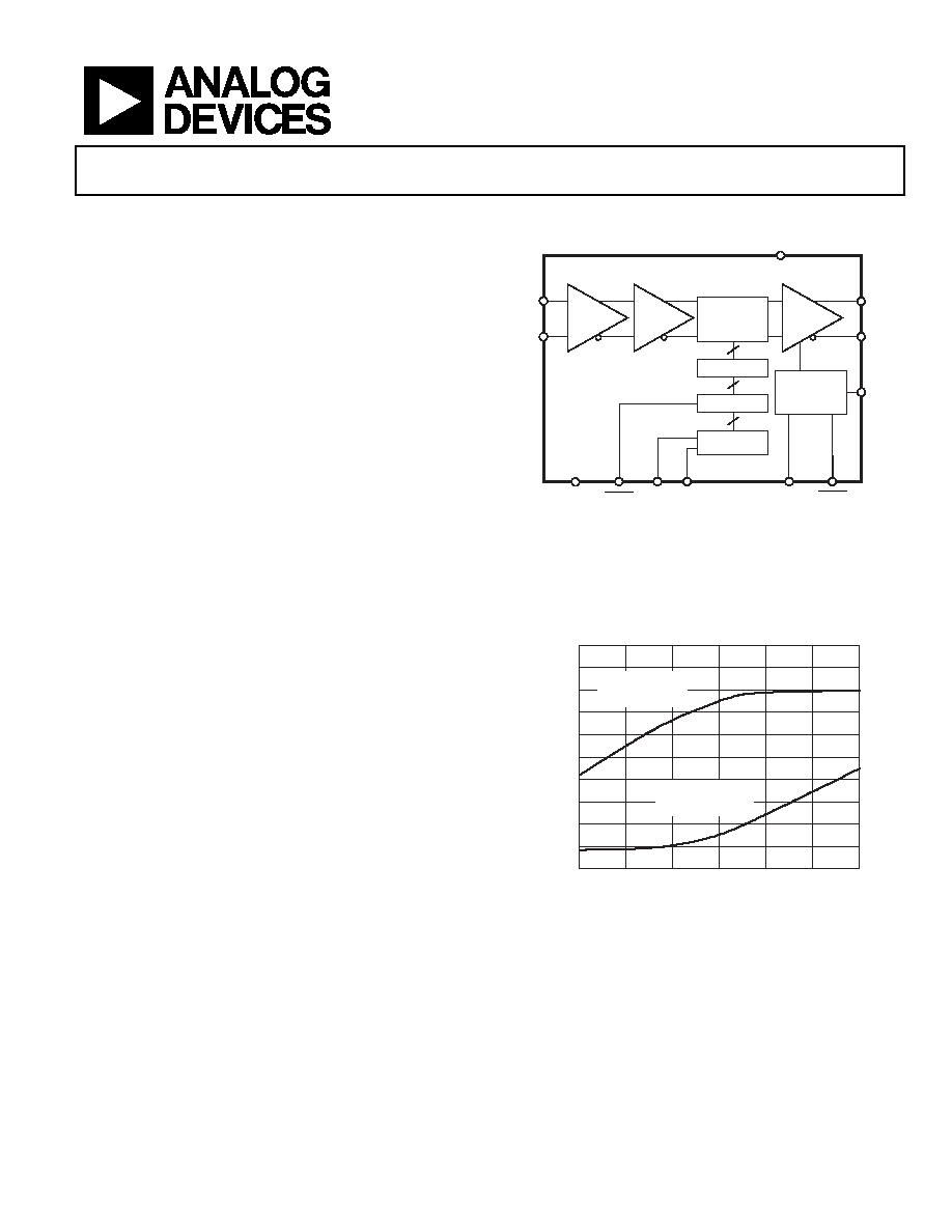
FUNCTIONAL BLOCK DIAGRAM
DIFF
OR
SINGLE
INPUT
AMP
8
AD8328
VIN+
VERNIER
BYP
GND
RAMP
POWER-DOWN
LOGIC
POWER
AMP
ATTENUATION
CORE
DECODE
DATA LATCH
SHIFT
REGISTER
VIN–
SDATA CLK
TXEN
03
158
-00
1
ZOUT DIFF =
300
VOUT–
VOUT+
ZIN (SINGLE) = 800
ZIN (DIFF) = 1.6k
DATEN
SLEEP
Figure 1.
GENERAL DESCRIPTION
The AD8328 is a low cost amplifier designed for coaxial line
driving. The features and specifications make the AD8328
ideally suited for MCNS-DOCSIS and EuroDOCSIS applications.
The gain of the AD8328 is digitally controlled. An 8-bit serial
word determines the desired output gain over a 59 dB range,
resulting in gain changes of 1 dB/LSB.
The AD8328 accepts a differential or single-ended input signal.
The output is specified for driving a 75 Ω load through a 2:1
transformer.
Distortion performance of 53 dBc is achieved with an output
level up to 60 dBmV at 65 MHz bandwidth over a wide
temperature range.
This device has a sleep mode function that reduces the quiescent
current to 2.6 mA and a full power-down function that reduces
power-down current to 20 μA.
The AD8328 is packaged in a low cost 20-lead LFCSP and
a 20-lead QSOP. The AD8328 operates from a single 5 V supply
and has an operational temperature range of 40°C to +85°C.
D
IS
T
OR
T
ION
(
d
B
c)
FREQUENCY (MHz)
–70
–68
–66
–64
–62
–60
–58
–56
–54
–52
–50
03
15
8-
0
02
VOUT = 60dBmV
@ MAX GAIN,
THIRD HARMONIC
VOUT = 60dBmV
@ MAX GAIN,
SECOND HARMONIC
5
1525
35
4555
65
Figure 2. Worst Harmonic Distortion vs. Frequency
相关PDF资料 |
PDF描述 |
|---|---|
| LT1675CGN#TR | IC MUX RGB TRIPLE 250MHZ 16SSOP |
| VI-J4D-MY-F4 | CONVERTER MOD DC/DC 85V 50W |
| ADV7524ABCBZ-1RL | IC TX HDMI/DVI LP |
| VI-J4D-MY-F2 | CONVERTER MOD DC/DC 85V 50W |
| VI-J4D-MY-F1 | CONVERTER MOD DC/DC 85V 50W |
相关代理商/技术参数 |
参数描述 |
|---|---|
| AD8328ARQZ-REEL | 制造商:Analog Devices 功能描述:SP Amp Line Driver Amp Single 5.25V 20-Pin QSOP T/R 制造商:Rochester Electronics LLC 功能描述:QSOP LOW COST +5V CABLE LINE DRIVER - Tape and Reel 制造商:Analog Devices 功能描述:IC,Digitally Controlled Gain Amplifier,SINGLE,SSOP,20PIN,PLASTIC |
| AD8330 | 制造商:AD 制造商全称:Analog Devices 功能描述:Low Cost, DC to 150 MHz Variable Gain Amplifier |
| AD8330_06 | 制造商:AD 制造商全称:Analog Devices 功能描述:Low Cost DC to 150 MHz Variable Gain Amplifier |
| AD8330_08 | 制造商:AD 制造商全称:Analog Devices 功能描述:Low Cost, DC to 150 MHz Variable Gain Amplifier |
| AD8330ACP | 制造商:AD 制造商全称:Analog Devices 功能描述:Low Cost DC-150 MHz Variable Gain Amplifier |
发布紧急采购,3分钟左右您将得到回复。