- 您现在的位置:买卖IC网 > PDF目录5772 > AD8330ACPZ-RL (Analog Devices Inc)IC AMP VGA 150MHZ LN LP 16LFCSP PDF资料下载
参数资料
| 型号: | AD8330ACPZ-RL |
| 厂商: | Analog Devices Inc |
| 文件页数: | 6/32页 |
| 文件大小: | 0K |
| 描述: | IC AMP VGA 150MHZ LN LP 16LFCSP |
| 标准包装: | 5,000 |
| 放大器类型: | 可变增益 |
| 电路数: | 1 |
| 输出类型: | 差分,满摆幅 |
| 转换速率: | 1500 V/µs |
| -3db带宽: | 150MHz |
| 电流 - 输入偏压: | 100nA |
| 电流 - 电源: | 20mA |
| 电压 - 电源,单路/双路(±): | 2.7 V ~ 6 V |
| 工作温度: | -40°C ~ 85°C |
| 安装类型: | 表面贴装 |
| 封装/外壳: | 16-VFQFN 裸露焊盘,CSP |
| 供应商设备封装: | 16-LFCSP-VQ |
| 包装: | 带卷 (TR) |
| 配用: | AD8330-EVALZ-ND - BOARD EVAL FOR AD8330 |
第1页第2页第3页第4页第5页当前第6页第7页第8页第9页第10页第11页第12页第13页第14页第15页第16页第17页第18页第19页第20页第21页第22页第23页第24页第25页第26页第27页第28页第29页第30页第31页第32页
AD8330
Data Sheet
Rev. F | Page 14 of 32
THEORY OF OPERATION
CIRCUIT DESCRIPTION
Many monolithic variable gain amplifiers use techniques that
share common principles that are broadly classified as translinear.
This term refers to circuit cells whose functions depend directly
on the very predictable properties of bipolar junction transistors,
notably the linear dependence of their transconductance on collec-
tor current. Since the discovery of these cells in 1967, and their
commercial exploitation in products developed during the early
1970s, accurate wide bandwidth analog multipliers, dividers,
and variable gain amplifiers have invariably employed translinear
principles.
Although these techniques are well understood, the realization
of a high performance variable gain amplifier (VGA) requires
special technologies and attention to many subtle details in
its design. The AD8330 is fabricated on a proprietary silicon-
on-insulator, complementary bipolar IC process and draws
on decades of experience in developing many leading edge
products using translinear principles to provide an unprecedented
level of versatility.
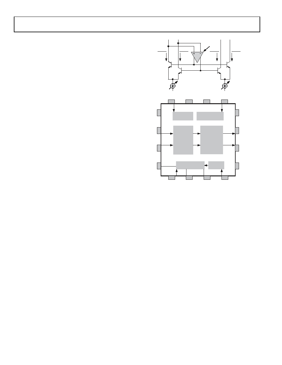
Figure 45 shows a basic representative cell comprising just four
transistors. This, or a very closely related form, is at the heart
of most translinear multipliers, dividers, and VGAs. The key
concepts are as follows:
First, the ratio of the currents in the left-hand and right-hand
pairs of transistors is identical, represented by the modulation
factor, x, with values between 1 and +1. Second, the input
signal is arranged to modulate the fixed tail current, ID, to cause
the variable value of x, introduced in the left-hand pair, to be
replicated in the right-hand pair, and, thus, generate the output
by modulating its nominally fixed tail current, IN. Third, the
current gain of this cell is exactly G = IN/ID over many decades
of variable bias current.
In practice, the realization of the full potential of this circuit
involves many other factors, but these three elementary ideas
remain essential.
By varying IN, the overall function is that of a two-quadrant
analog multiplier, exhibiting a linear relationship to both the
signal modulation factor (x) and this numerator current. On
the other hand, by varying ID, a two-quadrant analog divider
is realized, having a hyperbolic gain function with respect to
the input factor, x, controlled by this denominator current. The
AD8330 exploits both modes of operation. However, because a
hyperbolic gain function is generally of less value than one in
which the decibel gain is a linear function of a control input, a
special interface is included to provide either increasing or
decreasing exponential control of ID.
INPUT IS xlD
DENOMINATOR
BIAS CURRENT
ID
Q1
Q2
Q4
Q3
(1–x) ID
2
+
–
LOOP
AMPLIFIER
(1–x) IN
2
NUMERATOR
BIAS CURRENT
IN
OUTPUT IS xlN
G = IN/ID
(1+x) IN
2
(1–x) ID
2
03217-
046
Figure 45. Basic Core
COMM
OPHI
INLO
OPLO
INHI
VPSI
VPSO
CMOP
MODE
VDBS
CMGN
VMAG
OFST
R
T
N
C
L
B
N
E
VPOS
BIAS AND
VREF
GAIN INTERFACE
CM MODE AND
OFFSET CONTROL
OUTPUT
STAGES
OUTPUT
CONTROL
VGA CORE
AD8330
03217-
047
Figure 46. Block Schematic
Overall Structure
Figure 46 shows a block schematic of the AD8330 locating the
key sections. More detailed descriptions of its structure and
features are provided throughout the Theory of Operation
section; however, Figure 46 provides a general overview of its
capabilities.
The VGA core contains a more elaborate version of the cell
(linear-in-decibels) through the decibel gain interface at
Pin VDBS and its local common, Pin CMGN. The gain span
(that is, the decibel difference between maximum and
minimum values) provided by this control function is slightly
more than 50 dB. The absolute gain from input to output is a
function of source and load impedance, and depends on the
voltage on a second gain control pin (VMAG), explained in the
相关PDF资料 |
PDF描述 |
|---|---|
| 170M6559 | FUSE 550A 690V 3GKN/50 AR UC |
| 2027-9-SM-RP | GAS DISCHARGE TUBE |
| 170M6558 | FUSE 500A 690V 3GKN/50 AR UC |
| 3-1445055-2 | CONN HEADER 3MM 12POS R/A TIN |
| AD8330ARQZ-RL | IC AMP VGA 150MHZ LN LP 16QSOP |
相关代理商/技术参数 |
参数描述 |
|---|---|
| AD8330ARQ | 制造商:Analog Devices 功能描述:SP Amp Variable Gain Amp Single R-R O/P 6V 16-Pin QSOP Tube 制造商:Rochester Electronics LLC 功能描述:QSOP SINGLE VGA - Bulk 制造商:Analog Devices 功能描述:IC AMP DIFFERENTIAL |
| AD8330ARQ-REEL | 制造商:Analog Devices 功能描述:SP Amp Variable Gain Amp Single R-R O/P 6V 16-Pin QSOP T/R |
| AD8330ARQ-REEL7 | 制造商:Analog Devices 功能描述:SP Amp Variable Gain Amp Single R-R O/P 6V 16-Pin QSOP T/R |
| AD8330ARQZ | 功能描述:IC AMP VGA 150MHZ LN LP 16QSOP RoHS:是 类别:集成电路 (IC) >> Linear - Amplifiers - Instrumentation 系列:- 标准包装:2,500 系列:- 放大器类型:通用 电路数:4 输出类型:- 转换速率:0.6 V/µs 增益带宽积:1MHz -3db带宽:- 电流 - 输入偏压:45nA 电压 - 输入偏移:2000µV 电流 - 电源:1.4mA 电流 - 输出 / 通道:40mA 电压 - 电源,单路/双路(±):3 V ~ 32 V,±1.5 V ~ 16 V 工作温度:0°C ~ 70°C 安装类型:表面贴装 封装/外壳:14-TSSOP(0.173",4.40mm 宽) 供应商设备封装:14-TSSOP 包装:带卷 (TR) 其它名称:LM324ADTBR2G-NDLM324ADTBR2GOSTR |
| AD8330ARQZ-R7 | 功能描述:IC AMP VGA 150MHZ LN LP 16QSOP RoHS:是 类别:集成电路 (IC) >> Linear - Amplifiers - Instrumentation 系列:- 标准包装:50 系列:- 放大器类型:J-FET 电路数:2 输出类型:- 转换速率:3.5 V/µs 增益带宽积:1MHz -3db带宽:- 电流 - 输入偏压:30pA 电压 - 输入偏移:2000µV 电流 - 电源:200µA 电流 - 输出 / 通道:- 电压 - 电源,单路/双路(±):7 V ~ 36 V,±3.5 V ~ 18 V 工作温度:0°C ~ 70°C 安装类型:通孔 封装/外壳:8-DIP(0.300",7.62mm) 供应商设备封装:8-PDIP 包装:管件 |
发布紧急采购,3分钟左右您将得到回复。