参数资料
| 型号: | AD8335ACPZ-REEL |
| 厂商: | Analog Devices Inc |
| 文件页数: | 9/28页 |
| 文件大小: | 0K |
| 描述: | IC AMP VGA QUAD 64LFCSP |
| 产品变化通告: | AD8335 Metal Mask Change 12/Jul/2010 |
| 标准包装: | 2,500 |
| 系列: | X-AMP® |
| 类型: | 可变增益放大器 |
| 应用: | 信号处理 |
| 安装类型: | 表面贴装 |
| 封装/外壳: | 64-VFQFN 裸露焊盘,CSP |
| 供应商设备封装: | 64-LFCSP-VQ(9x9) |
| 包装: | 带卷 (TR) |
| 配用: | AD8335-EVALZ-ND - BOARD EVALUATION FOR AD8335 |
第1页第2页第3页第4页第5页第6页第7页第8页当前第9页第10页第11页第12页第13页第14页第15页第16页第17页第18页第19页第20页第21页第22页第23页第24页第25页第26页第27页第28页
Data Sheet
AD8335
Rev. B | Page 17 of 28
PREAMP
Although the preamp signal path is fully differential, the design is
optimized for single-ended input drive and signal source resistance
matching. Thus, the negative input to the differential preamplifier
PMDx pins must be ac-grounded to provide a balanced differential
signal at the PrA outputs. Detailed information regarding the
preamplifier architecture is found in the LNA section of the
The preamplifier consists of a fixed gain amplifier with differential
outputs. With the negative output available and a fixed gain of
8 (18.06 dB), an active input termination is synthesized by
connecting a feedback resistor between the negative output
and the positive input, Pin PIPx. This technique is well known
and results in the input resistance shown in Equation 2.
)
2
/
1
(
A
R
FB
IN
+
=
(2)
where A/2 is the single-ended gain, or the gain from the PIPx
inputs to the PONx outputs. Since the amplifier has a gain of ×8
from its input to its differential output, it is important to note
that the gain A/2 is the gain from Pin PIPx to Pin PONx, which
is 6 dB lower, or 12.04 dB (×4). The input resistance is reduced
by an internal bias resistor of 14.7 kΩ in parallel with the source
resistance connected to Pin PIPx, with Pin PMDx ac-grounded.
Equation 3 can be used to calculate the needed RFB for a desired
RIN, and is used for higher values of RIN.
kΩ
7
.
14
||
)
4
1
( +
=
FB
IN
R
(3)
For example, to set RIN = 200 Ω, the value of RFB is 1.013 kΩ. If the
simplified Equation 2 is used to calculate RIN, the value is 197 Ω,
resulting in a less than 0.1 dB gain error. Factors such as a widely
varying source resistance might influence the absolute gain
accuracy more significantly. At higher frequencies, the input
capacitance of the PrA needs to be considered. The user must
determine the level of matching accuracy and adjust RFB
accordingly.
The bandwidths (BW) of the preamplifier and VGA are
approximately 110 MHz each, resulting in a cascaded BW of
approximately 80 MHz. Ultimately the BW of the PrA limits the
accuracy of the synthesized RIN. For RIN = RS up to approximately
200 Ω, the best match is between 100 kHz and 10 MHz, where
the lower frequency limit is determined by the size of the ac
coupling capacitors, and the upper limit is determined by the
preamplifier BW. Furthermore, the input capacitance and RS
limits the BW at higher frequencies.
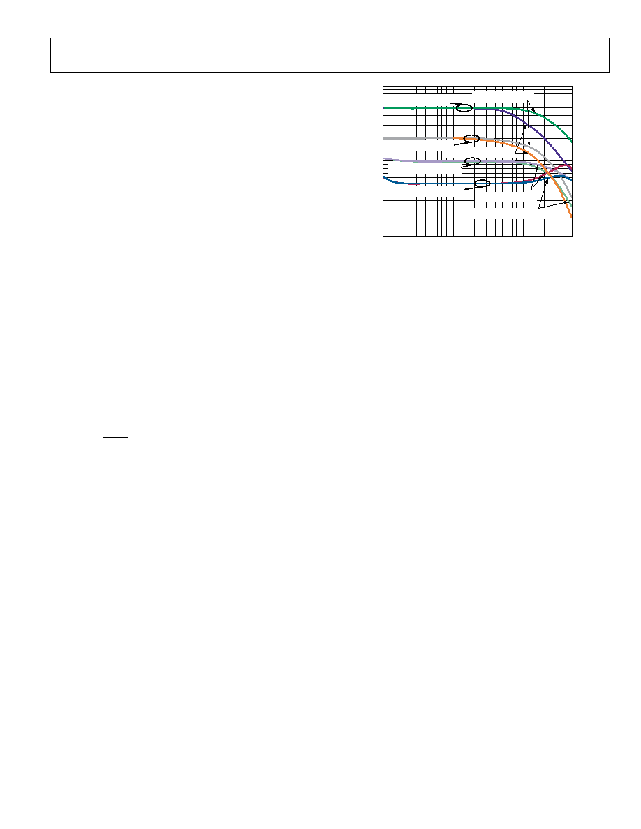
INP
U
T
I
M
P
E
DANC
E
(
)
FREQUENCY (Hz)
04
97
6
-10
2
10
100
1k
100k
1M
10M
50M
RIN = 500, RFB = 2.5k
RSH =
∞, CSH = 0pF
RIN = 200, RFB = 1k
RSH = 50, CSH = 22pF
RIN = 100, RFB = 499
RIN = 50, RFB = 249
RSH =
∞, CSH = 0pF
RSH = 50, CSH = 22pF
Figure 55. RIN vs. Frequency for Various Values of RFB;
Effects of RSH and CSH are also shown.
that at the lowest value, 50 Ω, RIN peaks at frequencies greater than
10 MHz. This is due to the BW roll-off of the PrA as mentioned
this peaking.
However, as can be seen for larger RIN values, parasitic capacitance
starts rolling off the signal BW before the PrA can produce
peaking and the RSH/CSH network further degrades the match.
Therefore, RSH and CSH should not be used for values of RIN
greater than 50 Ω.
Noise
The total input referred noise (IRN) is approximately 1.3 nV/√Hz.
Allowing for a gain of ×8 in the preamp, the VGA noise is
0.46 nV/√Hz referred to the PrA input. The preamp noise is
1.2 nV/√Hz. It is important to note that these noise values include
all amplifier noise sources, including the VGA and the preamplifier
gain resistors. Frequently, manufacturer noise specifications
exclude gain setting resistors, and the voltage noise spectral density
of an op amp might be presented as 1 nV/√Hz. Including the
gain resistors results in a much higher noise specification.
相关PDF资料 |
PDF描述 |
|---|---|
| LTC2751AIUHF-16#TRPBF | IC DAC 16BIT CUR OUT 38-QFN |
| AD8332ARUZ-R7 | IC AMP VAR GAIN 2CHAN 28TSSOP |
| VI-24J-IV-F3 | CONVERTER MOD DC/DC 36V 150W |
| AD8332ARUZ-RL | IC AMP VAR GAIN 2CHAN 28TSSOP |
| AD5328ARU | IC DAC 12BIT OCTAL W/BUF 16TSSOP |
相关代理商/技术参数 |
参数描述 |
|---|---|
| AD8335ACPZ-REEL7 | 功能描述:IC AMP VGA QUAD 64LFCSP RoHS:是 类别:集成电路 (IC) >> 线性 - 放大器 - 专用 系列:X-AMP® 产品培训模块:Lead (SnPb) Finish for COTS Obsolescence Mitigation Program 标准包装:60 系列:- 类型:可变增益放大器 应用:CATV 安装类型:表面贴装 封装/外壳:20-WQFN 裸露焊盘 供应商设备封装:20-TQFN-EP(5x5) 包装:托盘 |
| AD8335EVAL | 制造商:Analog Devices 功能描述:EVAL BOARD ((NS)) |
| AD8335-EVAL | 制造商:AD 制造商全称:Analog Devices 功能描述:Quad Low Noise, Low Cost Variable Gain Amplifier |
| AD8335-EVALZ | 功能描述:BOARD EVALUATION FOR AD8335 RoHS:是 类别:编程器,开发系统 >> 评估板 - 运算放大器 系列:X-AMP® 产品培训模块:Lead (SnPb) Finish for COTS Obsolescence Mitigation Program 标准包装:1 系列:- |
| AD8336 | 制造商:AD 制造商全称:Analog Devices 功能描述:General-Purpose, −55 to +125, Wide Bandwidth, DC-Coupled VGA |
发布紧急采购,3分钟左右您将得到回复。