- 您现在的位置:买卖IC网 > PDF目录373944 > AD8341-EVAL (Analog Devices, Inc.) 1.5 GHz to 2.4 GHz RF Vector Modulator PDF资料下载
参数资料
| 型号: | AD8341-EVAL |
| 厂商: | Analog Devices, Inc. |
| 元件分类: | 调制器/解调器 |
| 英文描述: | 1.5 GHz to 2.4 GHz RF Vector Modulator |
| 中文描述: | 1.5 GHz至2.4 GHz射频矢量调制器 |
| 文件页数: | 15/20页 |
| 文件大小: | 556K |
| 代理商: | AD8341-EVAL |
AD8341
Rev. 0 | Page 15 of 20
1RM
1AVG
A
SPAN 10MHz
1MHz/
CENTER 1.96Hz
–20
–12
–40
–50
–60
–70
–80
–90
–100
–112
MARKER 1 [T1 ]
–18.47dBm
1.95999900GHz
1
RBW 30kHz
VBW 100kHz
SWT 500ms
RF ATT 0dB
UNIT dBm
REF LVL
–12dBm
0
–30
0.3dB OFFSET
1 [T1]
1.95––4.06dBm
–77.64dBm
CH PWR
C11
C11
C0
C0
CU1
CU1
Figure 35. Output Spectrum, 1960 MHz, Single-Carrier CDMA2000
Test Model at 4 dBm, V
BBI
= V
BBQ
= 0.353 V, Adjacent Channel Power
Measured at ±2.25 MHz Carrier Offset in 1 MHz BW Input Signal Filtered
Using a Cavity Tuned Filter (Pass Band = 6.8 MHz)
Holding the differential I and Q control voltages steady at
0.353 V, input power was swept. Figure 36 shows variation in
spurious content, again measured at ±2.25 MHz carrier offset in
a 1 MHz bandwidth, as defined by the 3GPP2 specification.
0
–70
–90
–88
–86
–84
–82
–80
–78
–76
–74
–72
A
–20
–18
–16
–14
–12
–10
–8
–6
–4
–2
0
OUTPUT POWER (dBm)
Figure 36. Adjacent Channel Power vs. Output Power,
CDMA2000 Single Carrier @ 1960 MHz; ACP Measured at
±2.25 MHz Carrier Offset (1 MHz BW); V
BBI
= V
BBQ
= 0.353 V
With a fixed input power of 2.4 dBm, the output power was
again swept by exercising the I and Q inputs. V
BBI
and V
BBQ
were
kept equal and were swept from 100 mV to 500 mV. The result-
ing output power and ACP are shown in Figure 37.
0
0
–30
–25
–20
–15
–10
–5
O
0
0.1
0.2
0.3
0.4
0.5
IQ CONTROL VOLTAGE
–60
–65
–70
–75
–80
–85
–90
A
Figure 37. Output Power and ACP vs. I and Q Control Voltages,
CDMA2000 Test Model, V
BBI
= V
BBQ
, ACP Measured at
±2.25 MHz Carrier Offset in 1 MHz BW
Figure 37 shows that for a fixed input power, the ACP (measured in
dBm) tracks the output power as the gain is changed.
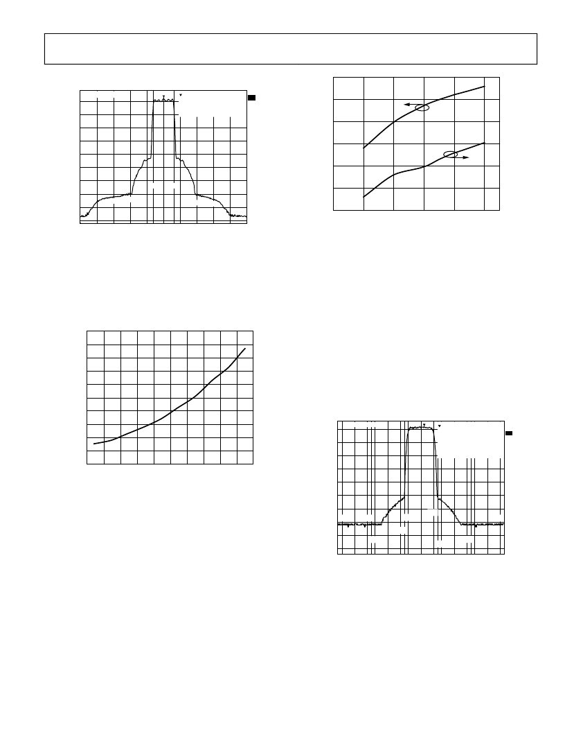
WCDMA APPLICATION
Figure 38 shows a plot of the output spectrum of the AD8341
transmitting a single-carrier WCDMA signal (Test Model 1-64
at 2140 MHz). The carrier power is approximately 9 dBm. The
differential I and Q control voltages are both equal to 0.353 V,
that is, the vector is sitting on the unit circle at 45°. At this
power level, an adjacent channel power ratio of 61 dBc is
achieved. The alternate channel power ratio of 72 dBc is
dominated by the noise floor of the AD8341.
1RM
SPAN 25MHz
2.5MHz/
CENTER 2.14GHz
–30
–24
–50
–60
–70
–80
–90
–100
–110
–120
–124
OFFSET 1dB
0
–40
A
MARKER 1 [T1 ]
–28.39dBm
2.14050000GHz
RBW 30kHz
VBW 300kHz
SWT 1s
RF ATT 0dB
UNIT dBm
REF LVL
–24dBm
1 [T1]
2.14––8.95dBm
–60.78dB
CH PWR
1
C12
C12
C11
C11
C0
C0
CU1
CU1
CU2
Figure 38. AD8341 Single-Carrier WCDMA Spectrum at 2140 MHz
Figure 39 shows how ACPR and noise vary with varying input
power (differential I and Q control voltages are held at 0.353 V).
At high power levels, both adjacent and alternate channel power
ratios increase sharply. As output power drops, adjacent and
alternate channel power ratios both reach minimums before the
measurement becomes dominated by the noise floor of the
AD8341. At this point, adjacent and alternate channel power
ratios become approximately equal.
相关PDF资料 |
PDF描述 |
|---|---|
| AD8341ACPZ-REEL72 | 1.5 GHz to 2.4 GHz RF Vector Modulator |
| AD8341ACPZ-WP1 | 1.5 GHz to 2.4 GHz RF Vector Modulator |
| AD8343ARU-REEL | ER 19C 19#6 SKT RECP LINE |
| AD8343 | DC-to-2.5 GHz High IP3 Active Mixer |
| AD8343-EVAL | DC-to-2.5 GHz High IP3 Active Mixer |
相关代理商/技术参数 |
参数描述 |
|---|---|
| AD8341-EVALZ | 制造商:Analog Devices 功能描述:EVAL BOARD - Bulk |
| AD8341XCP | 制造商:Analog Devices 功能描述:- Bulk |
| AD8342 | 制造商:AD 制造商全称:Analog Devices 功能描述:Active Receive Mixer LF to 500 MHz |
| AD8342ACPZ-R2 | 制造商:Analog Devices 功能描述:UP/DOWN CONV MIXER 5V 2.4GHZ 16LFCSP EP - Tape and Reel |
| AD8342ACPZ-REEL7 | 功能描述:IC MIXER SIGE 500MHZ 16LFCSP RoHS:是 类别:RF/IF 和 RFID >> RF 混频器 系列:AD8342 产品培训模块:Lead (SnPb) Finish for COTS Obsolescence Mitigation Program 标准包装:100 系列:- RF 型:W-CDMA 频率:2.11GHz ~ 2.17GHz 混频器数目:1 增益:17dB 噪音数据:2.2dB 次要属性:- 电流 - 电源:11.7mA 电源电压:2.7 V ~ 3.3 V 包装:托盘 封装/外壳:12-VFQFN 裸露焊盘 供应商设备封装:12-QFN-EP(3x3) |
发布紧急采购,3分钟左右您将得到回复。