- 您现在的位置:买卖IC网 > PDF目录373944 > AD8341ACPZ-WP1 (ANALOG DEVICES INC) 1.5 GHz to 2.4 GHz RF Vector Modulator PDF资料下载
参数资料
| 型号: | AD8341ACPZ-WP1 |
| 厂商: | ANALOG DEVICES INC |
| 元件分类: | 无绳电话/电话 |
| 英文描述: | 1.5 GHz to 2.4 GHz RF Vector Modulator |
| 中文描述: | TELECOM, CELLULAR, RF AND BASEBAND CIRCUIT, QCC24 |
| 封装: | 4 X 4 MM, LEAD FREE, MO-220VGGD-2, LFCSP-24 |
| 文件页数: | 14/20页 |
| 文件大小: | 556K |
| 代理商: | AD8341ACPZ-WP1 |
AD8341
The 3 dB bandwidth is set by choosing C
FLT
according to the
following equation:
Rev. 0 | Page 14 of 20
pF
0.5
nF
10
kHz
45
C
f
3dB
+
×
≈
FLT
This equation has been verified for values of C
FLT
from 10 pF to
0.1 μF (bandwidth settings of approximately 4.5 kHz to 43 MHz).
INTERFACING TO HIGH SPEED DACs
The AD977x family of dual DACs is well suited to driving the I
and Q vector controls of the AD8341. While these inputs can in
general be driven by any DAC, the differential outputs and bias
level of the ADI TxDAC family allows for a direct connection
between DAC and modulator.
The AD977x family of dual DACs has differential current out-
puts. The full-scale current is user programmable and is usually
set to 20 mA, that is, each output swings from 0 mA to 20 mA.
The basic interface between the AD9777 DAC outputs and the
AD8341 I and Q inputs is shown in Figure 33. The Resistors R1
and R2 set the dc bias level according to the equation:
Bias Level
=
Average Output Current
×
R1
For example, if the full-scale current from each output is 20 mA,
each output will have an average current of 10 mA. Therefore to
set the bias level to the recommended 0.5 V, R1 and R2 should
be set to 50 each. R1 and R2 should always be equal.
If R3 is omitted, this will result in an available swing from
the DAC of 2 V p-p differential, which is twice the maximum
voltage range required by the AD8341. DAC resolution can be
maximized by adding R3, which scales down this voltage
according to the following equation:
=
Swing
Scale
Full
(
)
(
)
+
×
+
×
R3
R2
R2
R3
R2
R1
I
MAX
1
||
2
OPTIONAL
LOW-PASS
FILTER
0
R1
R2
R3
I
OUTB2
I
OUTA2
QBBM
QBBP
I
OUTB1
I
OUTA1
IBBM
IBBP
AD9777
AD8341
OPTIONAL
LOW-PASS
FILTER
R1
R2
R3
Figure 33. Basic AD9777 to AD8341 Interface
0
(
)
130
50 55 60 65 70 75 80 85 90
100 105
115 120
110
125
95
D
1.15
1.13
1.08
1.05
1.10
1.00
0.97
1.02
0.95
0.92
0.88
0.85
0.90
0.77
0.75
0.72
0.80
0.82
0.70
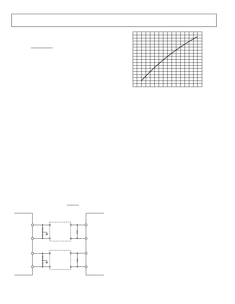
Figure 34. Peak-to-Peak DAC Output Swing vs.
Swing Scaling Resistor R3 (R1 = R2 = 50 )
Figure 34 shows the relationship between the value of R3 and
the peak baseband voltage with R1 and R2 equal to 50 .
From Figure 34, it can be seen that a value of 100 for R3 will
provide a peak-to-peak swing of 1 V p-p differential into the
AD8341’s I and Q inputs.
When using a DAC, low-pass image reject filters are typically
used to eliminate the Nyquist images produced by the DAC.
They also provide the added benefit of eliminating broadband
noise that might feed into the modulator from the DAC.
CDMA2000 APPLICATION
To test the compliance to the CDMA2000 base station standard,
a single-carrier CDMA2000 test model signal (forward pilot,
sync, paging, and six traffic as per 3GPP2 C.S0010-B, Table
6.5.2.1) was applied to the AD8341 at 1960 MHz. A cavity tuned
filter was used to reduce noise from the signal source being
applied to the device. The 6.8 MHz pass band of this filter is
apparent in the subsequent spectral plots.
Figure 35 shows a plot of the spectrum of the output signal
under nominal conditions. P
OUT
is equal to 4 dBm and V
BBI
=
V
BBQ
= 0.353 V, i.e., V
IBBP
V
IBBM
= V
QBBP
V
QBBM
= 0.353 V.
Noise and distortion is measured in a 1 MHz bandwidth at
±2.25 MHz carrier offset (30 kHz measurement bandwidth).
相关PDF资料 |
PDF描述 |
|---|---|
| AD8343ARU-REEL | ER 19C 19#6 SKT RECP LINE |
| AD8343 | DC-to-2.5 GHz High IP3 Active Mixer |
| AD8343-EVAL | DC-to-2.5 GHz High IP3 Active Mixer |
| AD8343ARU | DC-to-2.5 GHz High IP3 Active Mixer |
| AD8343ARU-REEL7 | DC-to-2.5 GHz High IP3 Active Mixer |
相关代理商/技术参数 |
参数描述 |
|---|---|
| AD8341-EVAL | 制造商:Analog Devices 功能描述:RF VECTOR MODULATOR 700 - 1000MHZ - Bulk |
| AD8341-EVALZ | 制造商:Analog Devices 功能描述:EVAL BOARD - Bulk |
| AD8341XCP | 制造商:Analog Devices 功能描述:- Bulk |
| AD8342 | 制造商:AD 制造商全称:Analog Devices 功能描述:Active Receive Mixer LF to 500 MHz |
| AD8342ACPZ-R2 | 制造商:Analog Devices 功能描述:UP/DOWN CONV MIXER 5V 2.4GHZ 16LFCSP EP - Tape and Reel |
发布紧急采购,3分钟左右您将得到回复。