- 您现在的位置:买卖IC网 > PDF目录373944 > AD8343ARU-REEL (ANALOG DEVICES INC) ER 19C 19#6 SKT RECP LINE PDF资料下载
参数资料
| 型号: | AD8343ARU-REEL |
| 厂商: | ANALOG DEVICES INC |
| 元件分类: | 衰减器 |
| 英文描述: | ER 19C 19#6 SKT RECP LINE |
| 中文描述: | 0 MHz - 2500 MHz RF/MICROWAVE DOUBLE BALANCED MIXER |
| 封装: | PLASTIC, TSSOP-14 |
| 文件页数: | 14/27页 |
| 文件大小: | 394K |
| 代理商: | AD8343ARU-REEL |
第1页第2页第3页第4页第5页第6页第7页第8页第9页第10页第11页第12页第13页当前第14页第15页第16页第17页第18页第19页第20页第21页第22页第23页第24页第25页第26页第27页
REV. 0
AD8343
–14–
SINGLE-ENDED-
TO-DIFFERENTIAL
CONVERSION
INPUT MATCHING
NETWORK
CORE BIAS NETWORK
SINGLE-ENDED-
TO-DIFFERENTIAL
CONVERSION
SINGLE-ENDED
INPUT SIGNAL
SINGLE-ENDED
LO INPUT SIGNAL
BIAS
CELL
CORE
AD8343
VPOS
DCPL
PWDN
LOIP
LOIM
INPP
INPM
OUTM
OUTP
COMM
LO
DRIVER
SINGLE-ENDED
OUTPUT SIGNAL
OUTPUT MATCHING
NETWORK
CORE BIAS
NETWORK
DIFFERENTIAL-
TO-
SINGLE-ENDED
CONVERSION
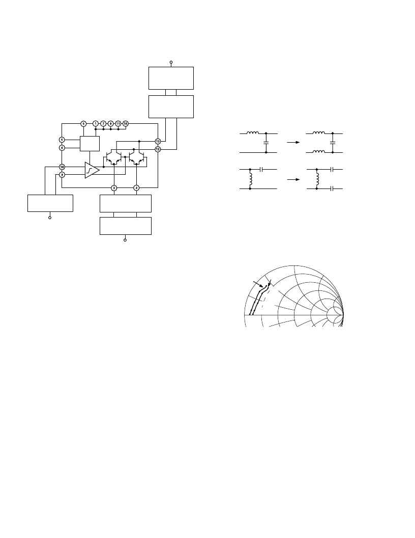
Figure 7. Basic AC Signal Connection Diagram
INPUT INTERFACE (INPP AND INPM)
Single-Ended-to-Differential Conversion
The AD8343 is designed to accept differential input signals for
best performance. While a single-ended input can be applied,
the signal capacity is reduced by 6 dB. Further, there would be
no cancellation of even-order distortion arising from the nonlin-
ear input impedances, so the effective signal handling capacity
will be reduced even further in distortion-sensitive situations.
That is, the intermodulation intercepts are degraded.
For these reasons it is strongly recommended that differential
signals be presented to the AD8343’s input. In addition to com-
mercially available baluns, there are various discrete and printed
circuit elements that can produce the required balanced wave-
forms and impedance match (i.e., rat-race baluns). These
alternate circuits can be employed to further reduce the compo-
nent cost of the mixer.
Baluns implemented in transmission line form (also known as
common-mode chokes) are useful up to frequencies of around
1 GHz, but are often excessively lossy at the highest frequencies
that the AD8343 can handle. M/A-Com manufactures these
baluns with their ETC line. Murata produces a true surface-
mount balun with their LDB20C series. Coilcraft and Toko are
also manufacturers of RF baluns.
Input Matching Considerations
The design of the input matching network should be undertaken
with two goals in mind: matching the source impedance to the
input impedance of the AD8343 and providing a dc bias current
path for the bias setting resistors.
The maximum power transfer into the device will occur when
there is a conjugate impedance match between the signal source
and the input of the AD8343. This match can be achieved with
the differential equivalent of the classic “L” network, as illustrated
in Figure 8. The figure gives two examples of the transformation
from a single-ended “L” network to its differential counterpart.
The design of “L” matching networks is adequately covered in
texts on RF amplifier design (for example: “Microwave Transis-
tor Amplifiers” by Guillermo Gonzalez).
L1
C1
L1/2
C1
L1/2
C2
L2
L2
2C2
2C2
SINGLE-ENDED
DIFFERENTIAL
Figure 8. Single-Ended-to-Differential Transformation
Figure 9 shows the differential input impedance of the AD8343
at the pins of the device. The two measurements shown in the
figure are for two different core currents set by resistors R3 and
R4; the real value impedance shift is caused by the change in tran-
sistor r
E
due to the change in current. The standard S parameter
files are available at the ADI web site (www.analog.com).
FREQUENCY (50MHz
–
2500MHz)
50MHz
500MHz
1000MHz
1500MHz
2500MHz
134
68
Figure 9. Input Differential Impedance (INPP, INPM) for
Two Values of R3 and R4
Figure 9 provides a reasonable starting point for the design of
the network. However, the particular board traces and pads will
transform the input impedance at frequencies in excess of about
500 MHz. For this reason it is best to make a
differential
input
impedance measurement at the board location where the match-
ing network will be installed, as a starting point for designing an
accurate matching network.
Differential impedance measurement is made relatively easy
through the use of a technique presented in an article by Lutz
Konstroffer in
RF Design
, January 1999, entitled “Finding the
Reflection Coefficient of a Differential One-Port Device.” This
article presents a mathematical formula for converting from a
two-port single-ended measurement to differential impedance.
A full two-port measurement is performed using a vector network
analyzer with Port 1 and Port 2 connected to the two differential
inputs of the device at the desired measurement plane. The two-
port measurement results are then processed with Konstroffer’s
formula (following), which is straightforward and can be imple-
mented through most RF design packages that can read and
analyze network analyzer data.
相关PDF资料 |
PDF描述 |
|---|---|
| AD8343 | DC-to-2.5 GHz High IP3 Active Mixer |
| AD8343-EVAL | DC-to-2.5 GHz High IP3 Active Mixer |
| AD8343ARU | DC-to-2.5 GHz High IP3 Active Mixer |
| AD8343ARU-REEL7 | DC-to-2.5 GHz High IP3 Active Mixer |
| AD8344 | Active Receive Mixer 400 MHz to 1.2 GHz |
相关代理商/技术参数 |
参数描述 |
|---|---|
| AD8343ARU-REEL7 | 制造商:Analog Devices 功能描述:Up/Down Conv Mixer 5V 2.4GHz 14-Pin TSSOP T/R 制造商:Rochester Electronics LLC 功能描述:- Tape and Reel 制造商:Analog Devices 功能描述:IC ACTIVE MIXER HIGH IP3 |
| AD8343ARUZ | 功能描述:IC MIXER ACTIVE HI-IP3 14-TSSOP RoHS:是 类别:RF/IF 和 RFID >> RF 混频器 系列:AD8343 产品培训模块:Lead (SnPb) Finish for COTS Obsolescence Mitigation Program 标准包装:100 系列:- RF 型:W-CDMA 频率:2.11GHz ~ 2.17GHz 混频器数目:1 增益:17dB 噪音数据:2.2dB 次要属性:- 电流 - 电源:11.7mA 电源电压:2.7 V ~ 3.3 V 包装:托盘 封装/外壳:12-VFQFN 裸露焊盘 供应商设备封装:12-QFN-EP(3x3) |
| AD8343ARUZ | 制造商:Analog Devices 功能描述:IF Subsystem |
| AD8343ARUZ-REEL | 功能描述:IC MIXER ACTIVE HIGH IP3 14TSSOP RoHS:是 类别:RF/IF 和 RFID >> RF 混频器 系列:AD8343 产品培训模块:Lead (SnPb) Finish for COTS Obsolescence Mitigation Program 标准包装:100 系列:- RF 型:W-CDMA 频率:2.11GHz ~ 2.17GHz 混频器数目:1 增益:17dB 噪音数据:2.2dB 次要属性:- 电流 - 电源:11.7mA 电源电压:2.7 V ~ 3.3 V 包装:托盘 封装/外壳:12-VFQFN 裸露焊盘 供应商设备封装:12-QFN-EP(3x3) |
| AD8343ARUZ-REEL7 | 功能描述:IC MIXER ACTIVE HIGH IP3 14TSSOP RoHS:是 类别:RF/IF 和 RFID >> RF 混频器 系列:AD8343 产品培训模块:Lead (SnPb) Finish for COTS Obsolescence Mitigation Program 标准包装:100 系列:- RF 型:W-CDMA 频率:2.11GHz ~ 2.17GHz 混频器数目:1 增益:17dB 噪音数据:2.2dB 次要属性:- 电流 - 电源:11.7mA 电源电压:2.7 V ~ 3.3 V 包装:托盘 封装/外壳:12-VFQFN 裸露焊盘 供应商设备封装:12-QFN-EP(3x3) |
发布紧急采购,3分钟左右您将得到回复。