- 您现在的位置:买卖IC网 > PDF目录373944 > AD8344-EVAL (Analog Devices, Inc.) Active Receive Mixer 400 MHz to 1.2 GHz PDF资料下载
参数资料
| 型号: | AD8344-EVAL |
| 厂商: | Analog Devices, Inc. |
| 英文描述: | Active Receive Mixer 400 MHz to 1.2 GHz |
| 中文描述: | 有源接收混频器400 MHz到1.2 GHz的 |
| 文件页数: | 16/20页 |
| 文件大小: | 429K |
| 代理商: | AD8344-EVAL |
AD8344
Rev. 0 | Page 16 of 20
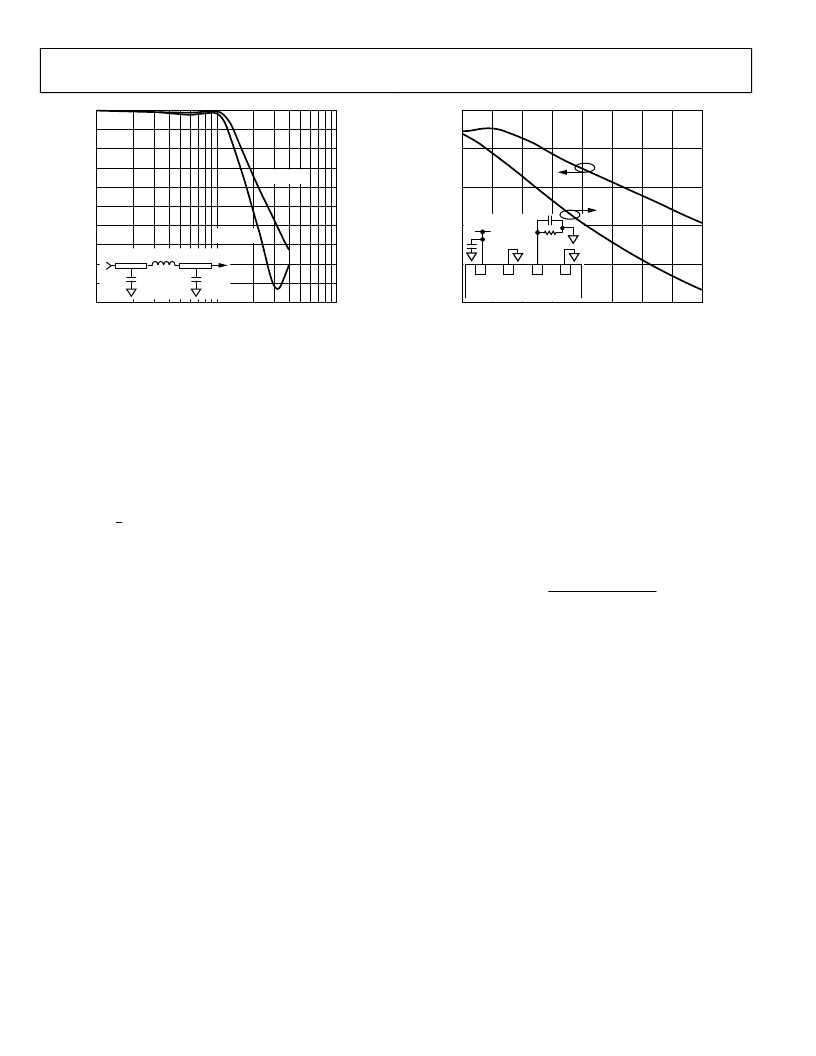
0
–50
–45
–40
–35
–30
–25
–20
–15
–10
–5
0.1
1
10
0
FREQUENCY (GHz)
R
IDEAL LPF
REAL LPF
4.7pF
4.7pF
6.8nH
Figure 43. Measured and Ideal LO Filter Frequency Response
BIAS RESISTOR SELECTION
An external bias resistor is used to set the dc current in the
mixer core. This provides the ability to reduce power consump-
tion at the expense of decreased dynamic range. Figure 44
shows the spurious-free dynamic range (SFDR) of the mixer for
a 1 Hz noise bandwidth versus the R
BIAS
resistor value. SFDR
was calculated using NF and IIP3 data collected at 900 MHz.
By definition,
(
)
)
B
(
10log
3
2
kT
NF
IIP3
SFDR
=
where
IIP3
is the input third-order intercept in dBm.
NF
is the
noise figure in dB.
kT
is the thermal noise power density and is
173.86 dBm/Hz at 298°K.
B
is the noise bandwidth in Hz.
In order to calculate the anticipated SFDR for a given applica-
tion, it is necessary to factor in the actual noise bandwidth. For
instance, if the IF noise bandwidth was 5 MHz, the anticipated
SFDR using a 2.43 k R
BIAS
would be 6.66 log10 (5 MHz) less
than the 1 Hz data in Figure 44 or ~80 dBc. Using a 2.43 k bias
resistor will set the quiescent power dissipation to ~415 mW for
a 5 V supply. If the R
BIAS
resistor value was raised to 3.9 k, the
SFDR for the same 5 MHz bandwidth would be reduced to
~77.5 dBc and the power dissipation would be reduced to
~335 mW In low power portable applications it may be advanta-
geous to reduce power consumption by using a larger value of R
BIAS
,
assuming reduced dynamic range performance is acceptable.
125
120
85
81
77
73
69
65
121
122
123
124
2.4
2.6
2.8
3.0
3.2
3.4
3.6
3.8
4.0
0
R
BIAS
(k
)
S
S
AD8344
COMM
9
EXRB
10
PWDN
11
VPDC
12
+V
S
R
BIAS
Figure 44. Impact of R
BIAS
Resistor Selection vs. Spurious-Free
Dynamic Range and Power Consumption,
F
RF
= 890 MHz and F
LO
= 1090 MHz
CONVERSION GAIN AND IF LOADING
The AD8344 is optimized for driving a 200 differential load.
Although the device is capable of driving a wide variety of
loads, in order to maintain optimum distortion and noise
performance, it is advised that the presented load at the IF
outputs is reasonably close to 200 . Figure 45 illustrates the
effect of IF loading on conversion gain. The mixer outputs
behave like Norton equivalent sources, where the conversion
gain is the effective transconductance of the mixer multiplied
by the loading impedance. The linear differential voltage
conversion gain of the mixer can be modeled as
RF
m
m
37.70
LOAD
f
g
j
g
×
R
Av
×
×
+
×
×
=
1
0.46
where
R
LOAD
is the differential loading impedance.
g
m
is the
mixer transconductance and is equal to 4070/R
BIAS
.
f
RF
is the
frequency of the signal applied to the RF port in GHz.
Large impedance loads cause the conversion gain to increase,
resulting in a decrease in input linearity and allowable signal
swing. In order to maintain positive conversion gain and pre-
serve spurious-free dynamic range performance, the differential
load presented at the IF port should remain within a range of
~100 to 250 .
相关PDF资料 |
PDF描述 |
|---|---|
| AD8344ACPZ-REEL7 | Active Receive Mixer 400 MHz to 1.2 GHz |
| AD8344ACPZ-WP | Active Receive Mixer 400 MHz to 1.2 GHz |
| AD8345ARE-REEL | 250 MHz.1000 MHz Quadrature Modulator |
| AD8345ARE-REEL7 | 250 MHz.1000 MHz Quadrature Modulator |
| AD8345 | 250 MHz.1000 MHz Quadrature Modulator |
相关代理商/技术参数 |
参数描述 |
|---|---|
| AD8344-EVALZ | 功能描述:EVAL BOARD FOR AD8344 制造商:analog devices inc. 系列:- 零件状态:在售 类型:混频器 频率:400MHz ~ 1.2GHz 配套使用产品/相关产品:AD8344 所含物品:板 标准包装:1 |
| AD8345 | 制造商:AD 制造商全称:Analog Devices 功能描述:250 MHz.1000 MHz Quadrature Modulator |
| AD8345ARE | 功能描述:IC QUADRATURE MOD 250MHZ 16TSSOP RoHS:否 类别:RF/IF 和 RFID >> RF 调制器 系列:- 产品培训模块:Lead (SnPb) Finish for COTS Obsolescence Mitigation Program 标准包装:2,500 系列:- 功能:调制器 LO 频率:700MHz ~ 2.3GHz RF 频率:700MHz ~ 2.3GHz P1dB:1dBm 底噪:-148dBm/Hz 输出功率:-1dBm 电流 - 电源:46mA 电源电压:2.7 V ~ 3.6 V 测试频率:1.75GHz 封装/外壳:28-WFQFN 裸露焊盘 包装:带卷 (TR) |
| AD8345ARE-REEL | 制造商:Analog Devices 功能描述:Quadrature Mod 80MHz 16-Pin TSSOP EP T/R |
| AD8345ARE-REEL7 | 功能描述:IC QUADRATURE MOD 250MHZ 16TSSOP RoHS:否 类别:RF/IF 和 RFID >> RF 调制器 系列:- 产品培训模块:Lead (SnPb) Finish for COTS Obsolescence Mitigation Program 标准包装:2,500 系列:- 功能:调制器 LO 频率:700MHz ~ 2.3GHz RF 频率:700MHz ~ 2.3GHz P1dB:1dBm 底噪:-148dBm/Hz 输出功率:-1dBm 电流 - 电源:46mA 电源电压:2.7 V ~ 3.6 V 测试频率:1.75GHz 封装/外壳:28-WFQFN 裸露焊盘 包装:带卷 (TR) |
发布紧急采购,3分钟左右您将得到回复。