- 您现在的位置:买卖IC网 > PDF目录373944 > AD8346ARU (ANALOG DEVICES INC) 0.8 GHz-2.5 GHz Quadrature Modulator PDF资料下载
参数资料
| 型号: | AD8346ARU |
| 厂商: | ANALOG DEVICES INC |
| 元件分类: | 衰减器 |
| 英文描述: | 0.8 GHz-2.5 GHz Quadrature Modulator |
| 中文描述: | 800 MHz - 2500 MHz RF/MICROWAVE I/Q MODULATOR |
| 封装: | TSSOP-16 |
| 文件页数: | 8/12页 |
| 文件大小: | 190K |
| 代理商: | AD8346ARU |
REV. 0
AD8346
–8–
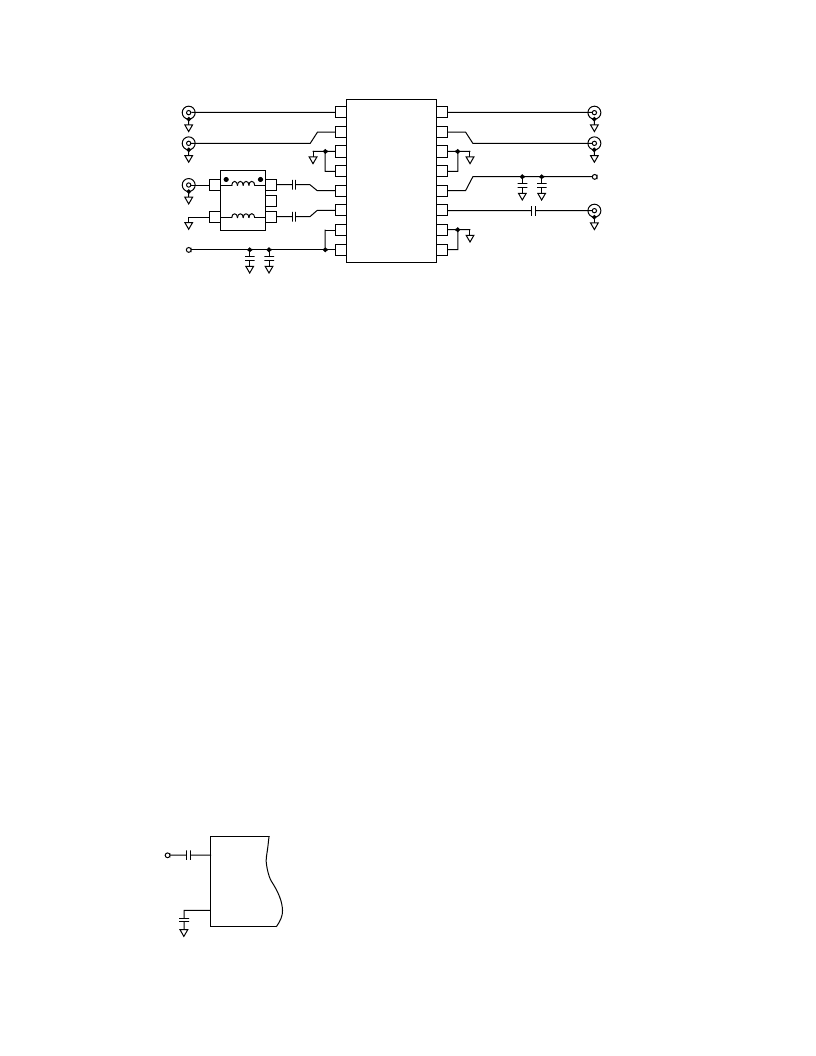
Basic Connections
The basic connections for operating the AD8346 are shown in
Figure 21. A single power supply of between 2.7 V and 5.5 V is
applied to pins VPS1 and VPS2. A pair of ESD protection
diodes are connected internally between VPS1 and VPS2 so
these must be tied to the same potential. Both pins should be
individually decoupled using 100 pF and 0.01
μ
F capacitors,
located as close as possible to the device. For normal operation,
the enable pin, ENBL, must be pulled high. The turn-on threshold
for ENBL is 2 V. To put the device in its power-down mode,
ENBL must be pulled below 0.5 V. Pins COM1 to COM4
should all be tied to a low impedance ground plane.
The I and Q ports should be driven differentially. This is conve-
nient as most modern high speed DACs have differential out-
puts. For optimal performance, the drive signal should be a
2 V p-p (differential) signal with a bias level of 1.2 V, that is,
each input swings from 0.7 V to 1.7 V. The I and Q inputs have
input impedances of 12 k
. By dc coupling the DAC to the
AD8346 and applying small offset voltages, the LO feedthrough
can be reduced to well below its nominal value of –42 dBm (see
Figure 7).
LO Drive
The return loss of the LO port is shown in Figure 13. No addi-
tional matching circuitry is required to drive this port from a
50
source. For maximum LO suppression at the output, a
differential LO drive is recommended. In Figure 21, this is
achieved using a balun (M/A-COM Part Number ETC1-1-13).
The output of the balun, is ac coupled to the LO inputs which
have a bias level about 800 mV below supply. An LO drive level
of between –6 dBm and –12 dBm is required. For optimal per-
formance, a drive level of –10 dBm is recommended although a
level of –6 dBm will result in more stable temperature perfor-
mance (see Figure 3). Higher levels will degrade linearity while
lower levels will tend to increase the noise floor.
LOIP
LOIN
AD8346
100pF
100pF
LO
Figure 22. Single-Ended LO Drive
The LO terminal can be driven single-ended as shown in Figure
22 at the expense of slightly higher LO feedthrough. LOIN is ac
coupled to ground using a capacitor and LOIP is driven through
a coupling capacitor from a (single-ended) 50
source (this
scheme could also be reversed with LOIP being ac-coupled to
ground).
RF Output
The RF output is designed to drive a 50
load but must be ac
coupled as shown in Figure 21. If the I and Q inputs are driven
in quadrature by 2 V p-p signals, the resulting output power will
be around –10 dBm (see Figure 2 for variation in output power
over frequency).
Interface to AD9761 TxDAC
Figure 23 shows a dc coupled current output DAC interface.
The use of dual integrated DACs such as the AD9761 with
specified
±
0.02 dB and
±
0.004 dB gain and offset matching
characteristics ensures minimum error contribution (over tem-
perature) from this portion of the signal chain. The use of a
precision thin-film resistor network sets the bias levels precisely,
to prevent the introduction of offset errors, which will increase
LO feedthrough. For instance, selecting resistor networks with
0.1% ratio matching characteristics will maintain 0.03 dB gain
and offset matching performance.
Using resistive division, the dc bias level at the I and Q inputs to
the AD8346 is set to approximately 1.2 V. The four current
outputs of the DAC each delivers a full-scale current of 10 mA,
giving a voltage swing of 0 V to 1 V (at the DAC output). This
results in a 0.5 V p-p swing at the I and Q inputs of the AD8346
(resulting in a 1 V p-p differential swing).
Note that the ratio matching characteristics of the resistive net-
work, as opposed to its absolute accuracy, is critical in preserv-
ing the gain and offset balance between the I and Q signal path.
By applying small dc offsets to the I and Q signals from the
DAC, the LO suppression can be reduced from its nominal
value of –42 dBm to as low as –60 dBm while holding to ap-
proximately –50 dBm over temperature (see Figure 7 for a plot
of LO feedthrough over temperature for an offset compensated
circuit.)
TxDAC is a registered trademark of Analog Devices, Inc.
QBBP
IBBI
AD8346
QBBN
IBBN
COM4
COM1
COM4
COM1
VPS2
LOIN
VOUT
LOIP
COM3
VPS1
COM2
ENBL
1
2
3
4
5
6
7
8
16
15
14
13
12
11
10
9
C4
0.01
m
F
C3
100pF
C6
100pF
C7
100pF
T1
ETC1-1-13
1
2
3
5
4
C2
0.01
m
F
C1
100pF
C5
100pF
IP
IN
LO
+V
S
QP
QN
+V
S
VOUT
Figure 21. Basic Connections
相关PDF资料 |
PDF描述 |
|---|---|
| AD8346ARU-REEL7 | 0.8 GHz-2.5 GHz Quadrature Modulator |
| AD8347ARU-REEL | 0.8 GHz-2.7 GHz Direct Conversion Quadrature Demodulator |
| AD8347 | 0.8 GHz-2.7 GHz Direct Conversion Quadrature Demodulator |
| AD8347-EVAL | 0.8 GHz-2.7 GHz Direct Conversion Quadrature Demodulator |
| AD8347ARU | 0.8 GHz-2.7 GHz Direct Conversion Quadrature Demodulator |
相关代理商/技术参数 |
参数描述 |
|---|---|
| AD8346ARU-REEL | 制造商:Analog Devices 功能描述:Quadrature Mod 70MHz 16-Pin TSSOP T/R 制造商:Analog Devices 功能描述:QUADRATURE MOD 70MHZ 16TSSOP - Tape and Reel 制造商:Rochester Electronics LLC 功能描述:TSSOP DIRECT QUADRATURE MODULATOR - Tape and Reel |
| AD8346ARU-REEL7 | 功能描述:IC QUADRATURE MOD .8GHZ 16-TSSOP RoHS:否 类别:RF/IF 和 RFID >> RF 调制器 系列:- 产品培训模块:Lead (SnPb) Finish for COTS Obsolescence Mitigation Program 标准包装:2,500 系列:- 功能:调制器 LO 频率:700MHz ~ 2.3GHz RF 频率:700MHz ~ 2.3GHz P1dB:1dBm 底噪:-148dBm/Hz 输出功率:-1dBm 电流 - 电源:46mA 电源电压:2.7 V ~ 3.6 V 测试频率:1.75GHz 封装/外壳:28-WFQFN 裸露焊盘 包装:带卷 (TR) |
| AD8346ARUZ | 功能描述:IC QUADRATURE MOD .8GHZ 16-TSSOP RoHS:是 类别:RF/IF 和 RFID >> RF 调制器 系列:- 产品培训模块:Lead (SnPb) Finish for COTS Obsolescence Mitigation Program 标准包装:2,500 系列:- 功能:调制器 LO 频率:700MHz ~ 2.3GHz RF 频率:700MHz ~ 2.3GHz P1dB:1dBm 底噪:-148dBm/Hz 输出功率:-1dBm 电流 - 电源:46mA 电源电压:2.7 V ~ 3.6 V 测试频率:1.75GHz 封装/外壳:28-WFQFN 裸露焊盘 包装:带卷 (TR) |
| AD8346ARUZ | 制造商:Analog Devices 功能描述:IC, QUAD MODULATOR, 0.8-2.5GHZ, 16-TSSOP |
| AD8346ARUZ-REEL | 功能描述:IC MOD QUAD 2.5GHZ 16TSSOP RoHS:是 类别:RF/IF 和 RFID >> RF 调制器 系列:- 产品培训模块:Lead (SnPb) Finish for COTS Obsolescence Mitigation Program 标准包装:2,500 系列:- 功能:调制器 LO 频率:700MHz ~ 2.3GHz RF 频率:700MHz ~ 2.3GHz P1dB:1dBm 底噪:-148dBm/Hz 输出功率:-1dBm 电流 - 电源:46mA 电源电压:2.7 V ~ 3.6 V 测试频率:1.75GHz 封装/外壳:28-WFQFN 裸露焊盘 包装:带卷 (TR) |
发布紧急采购,3分钟左右您将得到回复。