- 您现在的位置:买卖IC网 > PDF目录18727 > AD8348ARUZ-REEL7 (Analog Devices Inc)IC QUADRATURE DEMOD 28-TSSOP TR PDF资料下载
参数资料
| 型号: | AD8348ARUZ-REEL7 |
| 厂商: | Analog Devices Inc |
| 文件页数: | 21/28页 |
| 文件大小: | 0K |
| 描述: | IC QUADRATURE DEMOD 28-TSSOP TR |
| 标准包装: | 1,000 |
| 功能: | 解调器 |
| LO 频率: | 100MHz ~ 2GHz |
| RF 频率: | 50MHz ~ 1GHz |
| P1dB: | -22dBm |
| 增益: | 25.5dB |
| 噪音数据: | 10.75dB |
| 电流 - 电源: | 58mA |
| 电源电压: | 2.7 V ~ 5.5 V |
| 封装/外壳: | 28-TSSOP(0.173",4.40mm 宽) |
| 供应商设备封装: | 28-TSSOP |
| 包装: | 带卷 (TR) |
第1页第2页第3页第4页第5页第6页第7页第8页第9页第10页第11页第12页第13页第14页第15页第16页第17页第18页第19页第20页当前第21页第22页第23页第24页第25页第26页第27页第28页
�� �
�
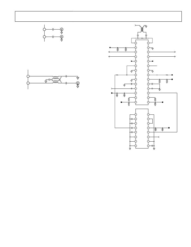
�AD8348�
�MXIN� 19�
�1000pF�
�MXIN�
�LO�
�4� 5�
�3� 1�
�1:1�
�MXIP� 18�
�MXIP�
�1000pF�
�60.4� ?�
�1000pF�
�1000pF�
�AD8348�
�Figure� 53.� Driving� the� MX� Inputs� from� a� Differential� Source�
�1�
�LOIP�
�LOIN� 28�
�+V� S�
�If� the� MX� inputs� are� to� be� driven� from� a� single-ended� 50� Ω� source,�
�a� 4:1� balun� can� be� used� to� transform� the� 200� Ω� impedance� of�
�the� inputs� to� 50� Ω� while� performing� the� required� single-ended-�
�0.1μF�
�TO� BASEBAND�
�I� ADC�
�100pF�
�2�
�3�
�4�
�VPOS1� COM1� 27�
�IOPN� QOPN� 26�
�IOPP� QOPP� 25�
�TO� BASEBAND�
�Q� ADC�
�to-differential� conversion.� The� recommended� transformer� is� the�
�M/A-COM� ETK4-2T.�
�V� REF�
�5�
�6�
�VCMO�
�IAIN�
�ENVG� 24�
�QAIN� 23�
�+V� S�
�7�
�COM3�
�COM3� 22�
�MXIN� 19�
�1000pF�
�1.02k� ?�
�8�
�IMXO�
�QMXO� 21�
�1.24k� ?�
�V� CMO�
�1μF�
�ETK4-2T�
�9�
�COM2� VPOS3� 20�
�100pF�
�0.1μF�
�+V� S�
�MXIP� 18�
�1000pF�
�MXIP�
�1000pF�
�10�
�IFIN�
�MXIN� 19�
�1000pF�
�Figure� 54.� Driving� the� MX� Inputs� from� a� Single-Ended� 50� Ω� Source�
�BASEBAND� OUTPUTS�
�IF� INPUT�
�Z� O� =� 200� ?�
�+V� S�
�0.1μF�
�1000pF�
�100pF�
�100pF�
�11�
�12�
�13�
�IFIP�
�VPOS2�
�IOFS�
�MXIP� 18�
�VGIN� 17�
�QOFS� 16�
�1000pF�
�100pF�
�The� baseband� amplifier� outputs,� IOPP,� IOPN,� QOPP,� and� QOPN,�
�V� REF�
�1000pF�
�14�
�VREF�
�ENBL� 15�
�100pF�
�+V� S�
�should� be� presented� with� loads� of� at� least� 2� k� (single-ended� to�
�ground).� They� are� not� designed� to� drive� 50� Ω� loads� directly.� The�
�AD8362�
�typical� swing� for� these� outputs� is� 2� V� p-p� differential� (1� V� p-p�
�1�
�COMM� ACOM� 16�
�single-ended),� but� larger� swings� are� possible� as� long� as� care� is� taken�
�to� ensure� that� the� signals� remain� within� the� lower� limit� of� 0.5� V�
�1μF�
�1μF�
�2�
�3�
�CHPF�
�DECL�
�VREF� 15�
�VTGT� 14�
�and� the� upper� limit� of� V� S� ?� 1� V� of� the� output� swing.� To� achieve�
�a� larger� swing,� it� is� necessary� to� adjust� the� common-mode� bias� of�
�1μF�
�1μF�
�4�
�INHI�
�VPOS� 13�
�100pF�
�0.1μF�
�+V� S�
�the� baseband� output� signals.� Increasing� the� swing� can� have� the�
�5�
�INLO�
�VOUT� 12�
�benefit� of� improving� the� signal-to-noise� ratio� of� the� baseband�
�6�
�DECL�
�VSET� 11�
�V� SET�
�amplifier� output.�
�7�
�PWDN� ACOM� 10�
�1μF�
�When� connecting� the� baseband� outputs� to� other� devices,� care�
�8�
�COMM�
�CLPF� 9�
�should� be� taken� to� ensure� that� the� outputs� are� not� capacitively�
�loaded� by� approximately� 20� pF� or� more.� Such� loads� could�
�potentially� overload� the� output� or� induce� oscillations.� The� effect�
�of� capacitive� loading� on� the� baseband� amplifier� outputs� can� be�
�mitigated� by� inserting� series� resistors� of� approximately� 200� Ω.�
�OUTPUT� DC� BIAS� LEVEL�
�The� dc� bias� of� the� mixer� outputs� and� the� baseband� amplifier�
�inputs� and� outputs� is� determined� by� the� voltage� that� is� driven�
�onto� the� VCMO� pin.� The� range� of� this� voltage� is� typically�
�between� 500� mV� and� 4� V� when� operating� with� a� 5� V� supply.�
�To� achieve� maximum� voltage� swing� from� the� baseband� amplifiers,�
�VCMO� should� be� driven� at� 2.25� V;� this� allows� a� swing� of� up� to�
�7� V� p-p� differential� (3.5� V� p-p� single-ended).�
�INTERFACING� TO� DETECTOR� FOR� AGC� OPERATION�
�The� AD8348� can� be� interfaced� with� a� detector� such� as� the�
�AD8362� rms-to-dc� converter� to� provide� an� automatic� signal-�
�leveling� function� for� the� baseband� outputs.�
�Figure� 55.� AD8362� Configuration� for� AGC� Operation�
�Assuming� the� I� and� Q� channels� have� the� same� rms� power,� the�
�mixer� output� (or� the� output� of� the� baseband� filter)� of� one� channel�
�can� be� used� as� the� input� of� the� AD8362.� The� AD8362� should� be�
�operated� in� a� region� where� its� linearity� error� is� small.� Also,� a�
�voltage� divider� should� be� implemented� with� an� external� resistor�
�in� series� with� the� 200� Ω� input� impedance� of� the� AD8362� input.�
�This� attenuates� the� AD8348� mixer� output� so� that� the� AD8362�
�input� is� not� overdriven.� The� size� of� the� resistor� between� the�
�mixer� output� and� the� AD8362� input� should� be� chosen� so� that�
�the� peak� signal� level� at� the� input� of� the� AD8362� is� about� 10� dB�
�less� than� the� approximately� 10� dBm� maximum� of� the� AD8362�
�dynamic� range.�
�The� other� side� of� the� AD8348� baseband� output� should� be�
�loaded� with� a� resistance� equal� to� the� series� resistance� of� the�
�attenuating� resistor� in� series� with� the� AD8362’s� 200� Ω� input�
�impedance.� This� resistor� should� be� tied� to� the� source� driving�
�VCMO� so� that� there� is� no� dc� drawn� from� the� mixer� output.�
�Rev.� A� |� Page� 21� of� 28�
�相关PDF资料 |
PDF描述 |
|---|---|
| D2VW-01-3M | MINIATURE BASIC SWITCH |
| D2VW-01-1M | MINIATURE BASIC SWITCH |
| GLEB07A1B | SWITCH SIDE-ROTRY SNAP SPDT |
| HUF75639G3 | MOSFET N-CH 100V 56A TO-247 |
| D2VW-01L02A-1MS | MINIATURE BASIC SWITCH |
相关代理商/技术参数 |
参数描述 |
|---|---|
| AD8348-EVAL | 制造商:Analog Devices 功能描述:AD8348ARU EVAL - Bulk |
| AD8348-EVALZ | 功能描述:BOARD EVAL FOR AD8348 RoHS:是 类别:编程器,开发系统 >> 评估演示板和套件 系列:* 标准包装:1 系列:PSoC® 主要目的:电源管理,热管理 嵌入式:- 已用 IC / 零件:- 主要属性:- 次要属性:- 已供物品:板,CD,电源 |
| AD8348XRU | 制造商:Analog Devices 功能描述:QUADRATURE MODULATOR X-GRADE - Rail/Tube |
| AD8348XXX | 制造商:AD 制造商全称:Analog Devices 功能描述:50-1000 MHz Quadrature Demodulator |
| AD8349 | 制造商:AD 制造商全称:Analog Devices 功能描述:400 MHz to 6 GHz Broadband Quadrature Modulator |
发布紧急采购,3分钟左右您将得到回复。