参数资料
| 型号: | AD8367ARU |
| 厂商: | Analog Devices Inc |
| 文件页数: | 4/24页 |
| 文件大小: | 0K |
| 描述: | IC AMP VGA 14TSSOP |
| 标准包装: | 1 |
| 系列: | X-AMP® |
| 放大器类型: | 可变增益 |
| 电路数: | 1 |
| -3db带宽: | 500MHz |
| 电流 - 输入偏压: | 27µA |
| 电流 - 电源: | 26mA |
| 电压 - 电源,单路/双路(±): | 2.7 V ~ 5.5 V |
| 工作温度: | -40°C ~ 85°C |
| 安装类型: | 表面贴装 |
| 封装/外壳: | 14-TSSOP(0.173",4.40mm 宽) |
| 供应商设备封装: | 14-TSSOP |
| 包装: | 管件 |
AD8367
Rev. A | Page 12 of 24
02710-029
50
Ω
VOUT
VB1
VB2
FROM
INTEGRATOR
Figure 29. A 50 Ω resistor is added to the
output to prevent package resonance.
POWER AND VOLTAGE METRICS
Although power is the traditional metric used in the analysis
of cascaded systems, most active circuit blocks fundamentally
respond to voltage. The relationship between power and voltage
is defined by the impedance level. When input and output
impedance levels are the same, power gain and voltage gain
are identical. However, when impedance levels change between
input and output, they differ. Thus, one must be very careful to
use the appropriate gain for system chain analyses. Quantities
such as OIP3 are quoted in dBV rms as well as dBm referenced
to 200 Ω. The dBV rms unit is defined as decibels relative to
1 V rms. In a 200 Ω environment, the conversion from dBV rms
to dBm requires the addition of 7 dB to the dBV rms value. For
example, a 2 dBV rms level corresponds to 9 dBm.
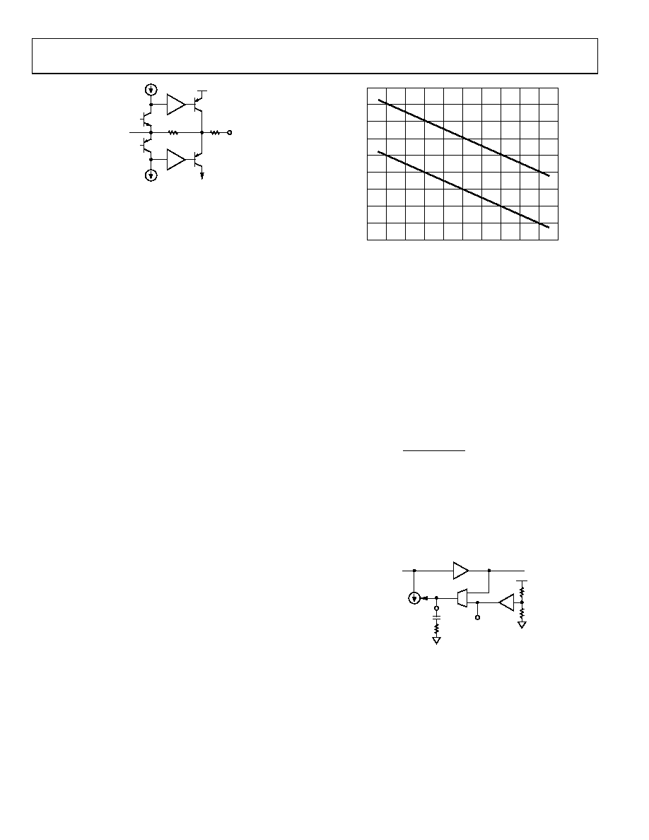
NOISE AND DISTORTION
Since the AD8367 consists of a passive variable attenuator
followed by a fixed gain amplifier, the noise and distortion
characteristics as a function of the gain voltage are easily
predicted. The input-referred noise increases in proportion to
the attenuation level. Figure 30 shows noise figure, NF, as a
function of VGAIN for the MODE pin pulled high. The minimum
NF of 7.5 dB occurs at maximum gain and increases 1 dB for
every 1 dB reduction in gain. In receiver applications, the
minimum NF should occur at the maximum gain where the
received signal presumably is weak. At higher levels, a lower
gain is needed, and the increased NF becomes less important.
The input-referred distortion varies in a similar manner to the
noise. Figure 30 illustrates how the third-order intercept point
at the input, IIP3, behaves as a function of VGAIN. The highest
IIP3 of 20 dBV rms (27 dBm re 200 Ω) occurs at minimum
gain. The IIP3 then decreases 1 dB for every 1 dB increase in
gain. At lower levels, a degraded IIP3 is acceptable. Overall, the
dynamic range, represented by the difference between IIP3 and
NF, remains reasonably constant as a function of gain. The
output distortion and compression are essentially independent
of the gain. At low gains, when the input level is high, input
overload can occur, causing premature distortion.
60
–30
–20
–10
0
10
20
30
40
50
60
–30
–20
–10
10
20
30
40
50
0
1.0
0.9
0.8
0.7
0.6
0.5
0.4
0.3
0.2
0.1
02710-030
VGAIN (V)
IIP3
(
d
BV)
NF
(dB)
NF
IIP3
Figure 30. Noise Figure and Input Third-Order Intercept vs.
Gain (RSOURCE = 200 Ω)
OUTPUT CENTERING
To maximize the ac swing at the output of the AD8367, the
output level is centered midway between ground and the supply.
This is achieved when the DECL pin is bypassed to ground via a
shunt capacitor. The loop acts to suppress deviations from the
reference at outputs below its corner frequency while not affect-
ing signals above it, as shown in Figure 31. The maximum
corner frequency with no external capacitor is 500 kHz. The
corner frequency can be lowered arbitrarily by adding an
external capacitor, CHP:
0.02
(nF)
10
(kHz)
+
=
HP
C
f
(3)
A 100 Ω in series with the CHP capacitor is recommended to
de-Q the resonant tank that is formed by the bond-wire
inductance and CHP. Failure to insert this capacitor can
potentially cause oscillations at higher frequencies at high
gain settings.
02710-031
MAIN
AMPLIFIER
gm
VOUT
FROM
INPUT
HPFL
CHP
RHP
VMID
DECL
AV = 1
Figure 31. The dc output level is centered to midsupply by a control loop
whose corner frequency is determined by CHP.
相关PDF资料 |
PDF描述 |
|---|---|
| AD8368ACPZ-WP | IC AMP VGA 24LFCSP |
| AD8369ARUZ-REEL7 | IC AMP VGA 16TSSOP |
| AD8370ARE-REEL7 | IC AMP VGA DIFF LN 16TSSOP |
| AD8372ACPZ-R7 | IC AMP VGA DIFF DUAL LN 32LFCSP |
| AD8375ACPZ-R7 | IC AMP VGA DIFF ULDIST 24LFCSP |
相关代理商/技术参数 |
参数描述 |
|---|---|
| AD8367ARU-REEL | 制造商:Analog Devices 功能描述: |
| AD8367ARU-REEL7 | 功能描述:IC AMP VGA 14TSSOP RoHS:否 类别:集成电路 (IC) >> Linear - Amplifiers - Instrumentation 系列:X-AMP® 标准包装:150 系列:- 放大器类型:音频 电路数:2 输出类型:- 转换速率:5 V/µs 增益带宽积:12MHz -3db带宽:- 电流 - 输入偏压:100nA 电压 - 输入偏移:500µV 电流 - 电源:6mA 电流 - 输出 / 通道:50mA 电压 - 电源,单路/双路(±):4 V ~ 32 V,±2 V ~ 16 V 工作温度:-40°C ~ 85°C 安装类型:表面贴装 封装/外壳:8-TSSOP(0.173",4.40mm 宽) 供应商设备封装:8-TSSOP 包装:管件 |
| AD8367ARU-REEL-7 | 制造商:AD 制造商全称:Analog Devices 功能描述:500 MHz, Linear-in-dB VGA with AGC Detector |
| AD8367ARUZ | 功能描述:IC AMP VGA 14TSSOP RoHS:是 类别:集成电路 (IC) >> Linear - Amplifiers - Instrumentation 系列:X-AMP® 标准包装:2,500 系列:- 放大器类型:通用 电路数:4 输出类型:- 转换速率:0.6 V/µs 增益带宽积:1MHz -3db带宽:- 电流 - 输入偏压:45nA 电压 - 输入偏移:2000µV 电流 - 电源:1.4mA 电流 - 输出 / 通道:40mA 电压 - 电源,单路/双路(±):3 V ~ 32 V,±1.5 V ~ 16 V 工作温度:0°C ~ 70°C 安装类型:表面贴装 封装/外壳:14-TSSOP(0.173",4.40mm 宽) 供应商设备封装:14-TSSOP 包装:带卷 (TR) 其它名称:LM324ADTBR2G-NDLM324ADTBR2GOSTR |
| AD8367ARUZ | 制造商:Analog Devices 功能描述:PROGRAMMABLE GAIN AMPLIFIER IC ((NW)) |
发布紧急采购,3分钟左右您将得到回复。