参数资料
| 型号: | AD8376ACPZ-R7 |
| 厂商: | Analog Devices Inc |
| 文件页数: | 7/24页 |
| 文件大小: | 0K |
| 描述: | IC AMP VGA DIFF DUAL 32LFCSP |
| 产品培训模块: | Differential Circuit Design Techniques for Communication Applications |
| 设计资源: | Using AD8376 to Drive Wide Bandwidth ADCs for High IF AC-Coupled Appls (CN0002) High Performance, Dual Channel IF Sampling Receiver (CN0140) |
| 标准包装: | 1 |
| 放大器类型: | 可变增益 |
| 电路数: | 2 |
| 输出类型: | 差分 |
| 转换速率: | 5000 V/µs |
| -3db带宽: | 700MHz |
| 电流 - 输入偏压: | 900nA |
| 电流 - 电源: | 250mA |
| 电压 - 电源,单路/双路(±): | 4.5 V ~ 5.5 V |
| 工作温度: | -40°C ~ 85°C |
| 安装类型: | 表面贴装 |
| 封装/外壳: | 32-VFQFN 裸露焊盘,CSP |
| 供应商设备封装: | 32-LFCSP-VQ(5x5) |
| 包装: | 标准包装 |
| 产品目录页面: | 775 (CN2011-ZH PDF) |
| 其它名称: | AD8376ACPZ-R7DKR |
Data Sheet
AD8376
Rev. B | Page 15 of 24
BROADBAND OPERATION
The AD8376 uses an open-collector output structure that
requires dc bias through an external bias network. Typically,
choke inductors are used to provide bias to the open-collector
outputs. Choke inductors work well at signal frequencies where
the impedance of the choke is substantially larger than the
target ac load impedance. In broadband applications, it may not
be possible to find large enough choke inductors that offer
enough reactance at the lowest frequency of interest while
offering a high enough self resonant frequency (SRF) to support
the maximum bandwidth available from the device. The circuit
in Figure 37 can be used when frequency response below
10 MHz is desired. This circuit replaces the bias chokes with
bias resistors. The bias resistor has the disadvantage of a greater
IR drop, and requires a supply rail that is several volts above the
local 5 V supply used to power the device. Additionally, it is
necessary to account for the ac loading effect of the bias
resistors when designing the output interface. Whereas the gain
should equal the optimum 150 Ω target load impedance to
provide the expected ac performance depicted in the data sheet.
Additionally, to ensure good output balance and even-order
distortion performance, it is essential that R1 = R2.
5
0.1F
50
ETC1-1-13
37.5
5V
SET TO
5V
R1
R2
VR
RL
A0 TO A4
1/2
AD8376
06725-
037
Figure 37. Single-Ended Broadband Operation with Resistive Pull-Ups
Using the formula for R1 (Equation 1), the values of R1 = R2
that provide a total presented load impedance of 150 Ω can be
found. The required voltage applied to the bias resistors, VR,
can be found by using the VR formula (Equation 2).
150
75
×
=
L
R
R1
(1)
and
5
10
40
3 +
×
=
R1
VR
(2)
For example, in the extreme case where the load is assumed to
be high impedance, RL = ∞, the equation for R1 reduces to R1 =
75 Ω. Using the equation for VR, the applied voltage should be
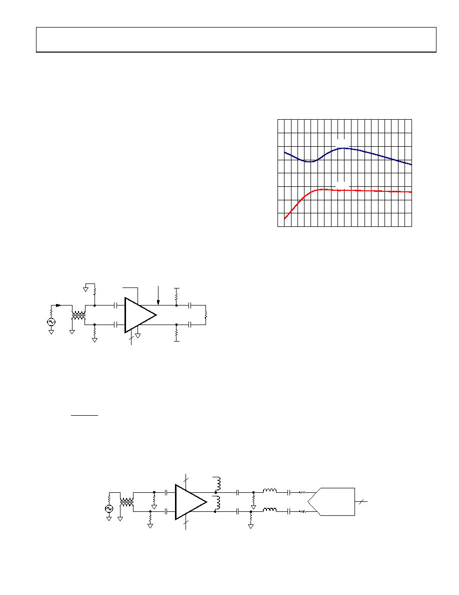
VR = 8 V. The measured single-tone low frequency harmonic
distortion for a 2 V p-p output using 75 Ω resistive pull-ups is
provided in Figure 38.
–80
–82
–84
–86
–88
–90
–92
–94
–96
HARM
O
NI
C
DI
S
T
O
RT
IO
N
(
d
Bc)
0
5
10
15
20
FREQUENCY (MHz)
HD2
HD3
06725-
038
Figure 38. Harmonic Distortion vs. Frequency Using Resistive Pull-Ups
ADC INTERFACING
The AD8376 is a high output linearity variable gain amplifier
that is optimized for ADC interfacing. The output IP3 and noise
floor essentially remain constant vs. the 24 dB available gain
range. This is a valuable feature in a variable gain receiver where
it is desirable to maintain a constant instantaneous dynamic
range as the receiver gain is modified. The output noise density
is typically around 20 nV/√Hz, which is comparable to 14-/16-
bit sensitivity limits. The two-tone IP3 performance of the
AD8376 is typically around 50 dBm. This results in SFDR levels
of better than 86 dB when driving the AD9445 up to 140 MHz.
There are several options available to the designer when using
the AD8376. The open-collector output provides the capability
of driving a variety of loads. Figure 39 shows a simplified wide-
band interface with the AD8376 driving a AD9445. The AD9445
is a 14-bit 125 MSPS analog-to-digital converter with a buffered
wideband input, which presents a 2 kΩ||3 pF differential load
impedance and requires a 2 V p-p differential input swing to
reach full scale.
0.1F
50
ETC1-1-13
37.5
0.1F
82
1H
5V
1H
5V
33
14
AD9445
14-BIT ADC
1/2
AD8376
5
B0 TO B4
A0 TO A4
06725-
039
L
(SERIES)
L
(SERIES)
VIN+
VIN–
Figure 39. Wideband ADC Interfacing Example Featuring of the AD8376 and the AD9445
相关PDF资料 |
PDF描述 |
|---|---|
| AD8390AACPZ-R2 | IC AMP DIFF LP LDIST 16LFCSP |
| AD8390ACPZ-REEL7 | IC AMP DIFF LP LDIST 16LFCSP |
| AD8397ARZ-REEL | IC OPAMP VF R-R DUAL LN 8SOIC |
| AD841SE | IC OPAMP GP 40MHZ 50MA 20CLCC |
| AD8420ARMZ-R7 | IC AMP INSTR RR 2.5KHZ 8MSOP |
相关代理商/技术参数 |
参数描述 |
|---|---|
| AD8376ACPZ-REEL7 | 制造商:AD 制造商全称:Analog Devices 功能描述:Ultra Low Distortion IF Dual VGA |
| AD8376ACPZ-WP | 制造商:Analog Devices 功能描述:ULTRALOW DISTORTION IF DUAL VGA - Gel-pak, waffle pack, wafer, diced wafer on film 制造商:Analog Devices 功能描述:IF CELLULAR DUAL DGA 制造商:Rochester Electronics LLC 功能描述: |
| AD8376-EVALZ | 制造商:Analog Devices 功能描述:EVALUATION BOARD - Bulk 制造商:Analog Devices 功能描述:EVALUATION BOARD ((NS)) |
| AD8380 | 制造商:AD 制造商全称:Analog Devices 功能描述:Fast, High-Voltage Drive, 6-Channel Output DecDriver Decimating LCD Panel Driver |
| AD8380JS | 制造商:Analog Devices 功能描述:LCD DRVR 3.3V/5V/12V/15V/18V 44-Pin MQFP |
发布紧急采购,3分钟左右您将得到回复。