- 您现在的位置:买卖IC网 > PDF目录10142 > AD8392AAREZ-RL (Analog Devices Inc)IC LINE DRVR ADSL/ADSL 28-TSSOP PDF资料下载
参数资料
| 型号: | AD8392AAREZ-RL |
| 厂商: | Analog Devices Inc |
| 文件页数: | 11/12页 |
| 文件大小: | 0K |
| 描述: | IC LINE DRVR ADSL/ADSL 28-TSSOP |
| 标准包装: | 2,500 |
| 类型: | 驱动器 |
| 驱动器/接收器数: | 2/0 |
| 规程: | xDSL |
| 电源电压: | 5 V ~ 24 V |
| 安装类型: | 表面贴装 |
| 封装/外壳: | 28-SOIC(0.173",4.40mm 宽)裸露焊盘 |
| 供应商设备封装: | 28-HTSSOP |
| 包装: | 带卷 (TR) |
AD8392A
Rev. 0 | Page 8 of 12
APPLICATIONS
SUPPLIES, GROUNDING, AND LAYOUT
The AD8392A can be powered from either single or dual
supplies, with the total supply voltage ranging from 10 V to
24 V. For optimum performance, a well regulated low ripple
supply should be used.
As with all high speed amplifiers, close attention should be paid
to supply decoupling, grounding, and overall board layout. Low
frequency supply decoupling should be provided with 10 μF
tantalum capacitors from each supply to ground. In addition, all
supply pins should be decoupled with 0.1 μF quality ceramic
chip capacitors placed as close as possible to the driver. An
internal low impedance ground plane should be used to provide
a common ground point for all driver and decoupling capacitor
ground requirements. Whenever possible, separate ground
planes should be used for analog and digital circuitry.
High speed layout techniques should be followed to minimize
parasitic capacitance around the inverting inputs. Some practical
examples of these techniques are keeping feedback traces as
short as possible and clearing away ground plane in the area of
the inverting inputs. Input and output traces should be kept
short and as far apart from each other as practical to avoid
crosstalk. When used as a differential driver, all differential
signal traces should be kept as symmetrical as possible.
POWER MANAGEMENT
The AD8392A can be configured in any of three active bias
states as well as a shutdown state via the use of two sets of
digitally programmable logic pins. Pin PD0 (1, 2) and Pin PD1
(1, 2) control Amplifier 1 and Amplifier 2, while PD0 (3, 4) and
Pin PD1 (3, 4) control Amplifier 3 and Amplifier 4. These pins
can be controlled directly with either 3.3 V or 5 V CMOS logic
by using the GND pins as a reference. If left unconnected, the
PD pins float low, placing the amplifier in the full bias mode.
Refer to the Specifications for the per amplifier quiescent
current for each of the available bias states.
As is shown in Figure 13, the AD8392A exhibits low output
impedance for the three active states. The shutdown state
(PD1, PD0 = 1, 1) provides a high impedance output.
THERMAL CONSIDERATIONS
When using a quad, high output current amplifier, such as the
AD8392A, special consideration should be given to system level
thermal design. In applications such as the ADSL/ADSL2+,
the AD8392A could be required to dissipate as much as 1.4 W
or more on-chip. Under these conditions, particular attention
should be paid to the thermal design to maintain safe operating
temperatures on the die. To aid in the thermal design, the
thermal information in the Thermal Resistance section can
be combined with what follows here.
JEDEC 4-layer board and a maximum die temperature of 150°C.
To provide additional guidance and design suggestions, a
thermal study was performed under a set of conditions more
closely aligned with an actual ADSL/ADSL2+ application.
In a typical ADSL/ADSL2+ line card, component density
usually dictates that most of the copper plane used for thermal
dissipation be internal. Additionally, each ADSL/ADSL2+ port
may be allotted only 1 square inch, or even less, of board space.
For these reasons, a special thermal test board was constructed
for this study. The 4-layer board measured approximately
4 inches × 4 inches and contained two internal 1 oz copper
ground planes, each measuring 2 inches × 3 inches. The top
layer contained signal traces and an exposed copper strip
inch × 3 inches to accommodate heat sinking, with no
other copper on the top or bottom of the board.
Three 28-lead TSSOPs were placed on the board representing
six ADSL channels, or one channel per square inch of copper,
with each channel dissipating 700 mW on-chip (1.4 W per
package). The die temperature is then measured in still air and
in a wind tunnel with calibrated airflow of 100 LFM, 200 LFM,
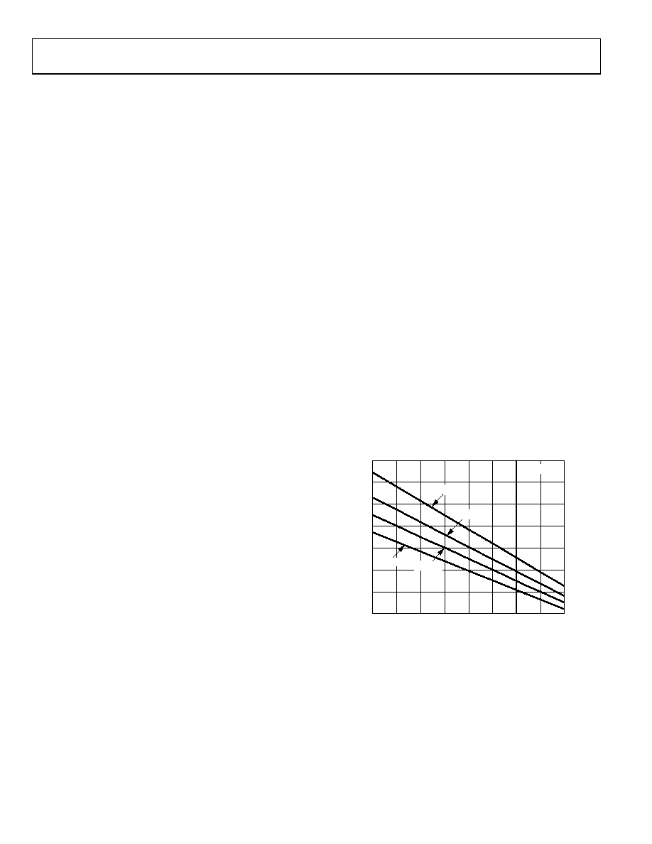
and 400 LFM. Figure 17 shows the power dissipation vs. the
ambient temperature for each airflow condition. The figure
assumes a maximum die temperature of 135°C. No heat sink
was used.
1.0
1.5
2.0
2.5
3.0
3.5
4.0
4.5
5
1525
354555657585
AMBIENT TEMPERATURE (°C)
P
O
W
E
R
DI
S
IP
AT
IO
N
(
W
)
TJ = 135°C
06
47
7-
0
51
STILL AIR
100LFM
200LFM
400LFM
Figure 17. Power Dissipation vs. Ambient
Temperature and Air Flow 28-Lead TSSOP/EP
This data is only provided as guidance to assist in the thermal
design process. Due diligence should be performed with regards
to power dissipation because there are many factors that can
affect thermal performance.
相关PDF资料 |
PDF描述 |
|---|---|
| AD7865BSZ-3REEL | IC ADC 14BIT 4CHAN 5V 44-MQFP |
| IDT7202LA50SO8 | IC FIFO ASYNCH 1KX9 35NS 28SOIC |
| VI-22K-IW-F2 | CONVERTER MOD DC/DC 40V 100W |
| VE-BN1-MW-F2 | CONVERTER MOD DC/DC 12V 100W |
| VI-22J-IX-B1 | CONVERTER MOD DC/DC 36V 75W |
相关代理商/技术参数 |
参数描述 |
|---|---|
| AD8392ACP-R2 | 制造商:Analog Devices 功能描述: 制造商:Rochester Electronics LLC 功能描述: |
| AD8392ACP-REEL | 制造商:Analog Devices 功能描述: |
| AD8392ACP-REEL7 | 制造商:Analog Devices 功能描述: 制造商:Rochester Electronics LLC 功能描述: |
| AD8392ACPZ-RL | 制造商:Analog Devices 功能描述:ADSL Driver Quad 40MHz 32-Pin LFCSP EP T/R 制造商:Analog Devices 功能描述:Dual Port ADSL/ADSL+Line Driver |
| AD8392ACPZ-RL7 | 制造商:Analog Devices 功能描述:ADSL Driver Quad 40MHz 32-Pin LFCSP EP T/R 制造商:Analog Devices 功能描述:ADSL DRVR QUAD 40MHZ 32LFCSP EP - Tape and Reel |
发布紧急采购,3分钟左右您将得到回复。