参数资料
| 型号: | AD8392AAREZ |
| 厂商: | Analog Devices Inc |
| 文件页数: | 7/12页 |
| 文件大小: | 0K |
| 描述: | IC ADSL/ADSL2 LINE DRVR 28-TSSOP |
| 标准包装: | 50 |
| 类型: | 驱动器 |
| 驱动器/接收器数: | 2/0 |
| 规程: | xDSL |
| 电源电压: | 5 V ~ 24 V |
| 安装类型: | 表面贴装 |
| 封装/外壳: | 28-SOIC(0.173",4.40mm 宽)裸露焊盘 |
| 供应商设备封装: | 28-HTSSOP |
| 包装: | 管件 |
AD8392A
Rev. 0 | Page 4 of 12
ABSOLUTE MAXIMUM RATINGS
Table 2.
Parameter
Rating
Supply Voltage
±13 V (+26 V)
Power Dissipation
See Figure 3
Storage Temperature Range
65°C to +150°C
Operating Temperature Range
40°C to +85°C
Lead Temperature (Soldering 10 sec)
300°C
Junction Temperature
150°C
Stresses above those listed under Absolute Maximum Ratings
may cause permanent damage to the device. This is a stress
rating only; functional operation of the device at these or any
other conditions above those indicated in the operational
section of this specification is not implied. Exposure to absolute
maximum rating conditions for extended periods may affect
device reliability.
THERMAL RESISTANCE
θJA is specified for the worst-case conditions, that is, θJA is specified
for the device soldered in the circuit board for surface-mount
packages.
Table 3.
Package Type
θJA
Unit
LFCSP-32 (CP)
27.27
°C/W
TSSOP-28/EP (RE)
35.33
°C/W
Maximum Power Dissipation
The power dissipated in the package (PD) is the sum of the
quiescent power dissipation and the power dissipated in the
package due to the load drive for all outputs. The quiescent
power is the voltage between the supply pins (VS) times the
quiescent current (IS). Assuming that the load (RL) is midsupply,
the total drive power is VS/2 × IOUT, some of which is dissipated
in the package and some in the load (VOUT × IOUT).
RMS output voltages should be considered. If RL is referenced
to VS as in single-supply operation, the total power is VS × IOUT.
In single supply with RL to VS, worst case is VOUT = VS/2.
Airflow increases heat dissipation, effectively reducing θJA. In
addition, more metal directly in contact with the package leads
from metal traces, through holes, ground, and power planes
reduces the θJA.
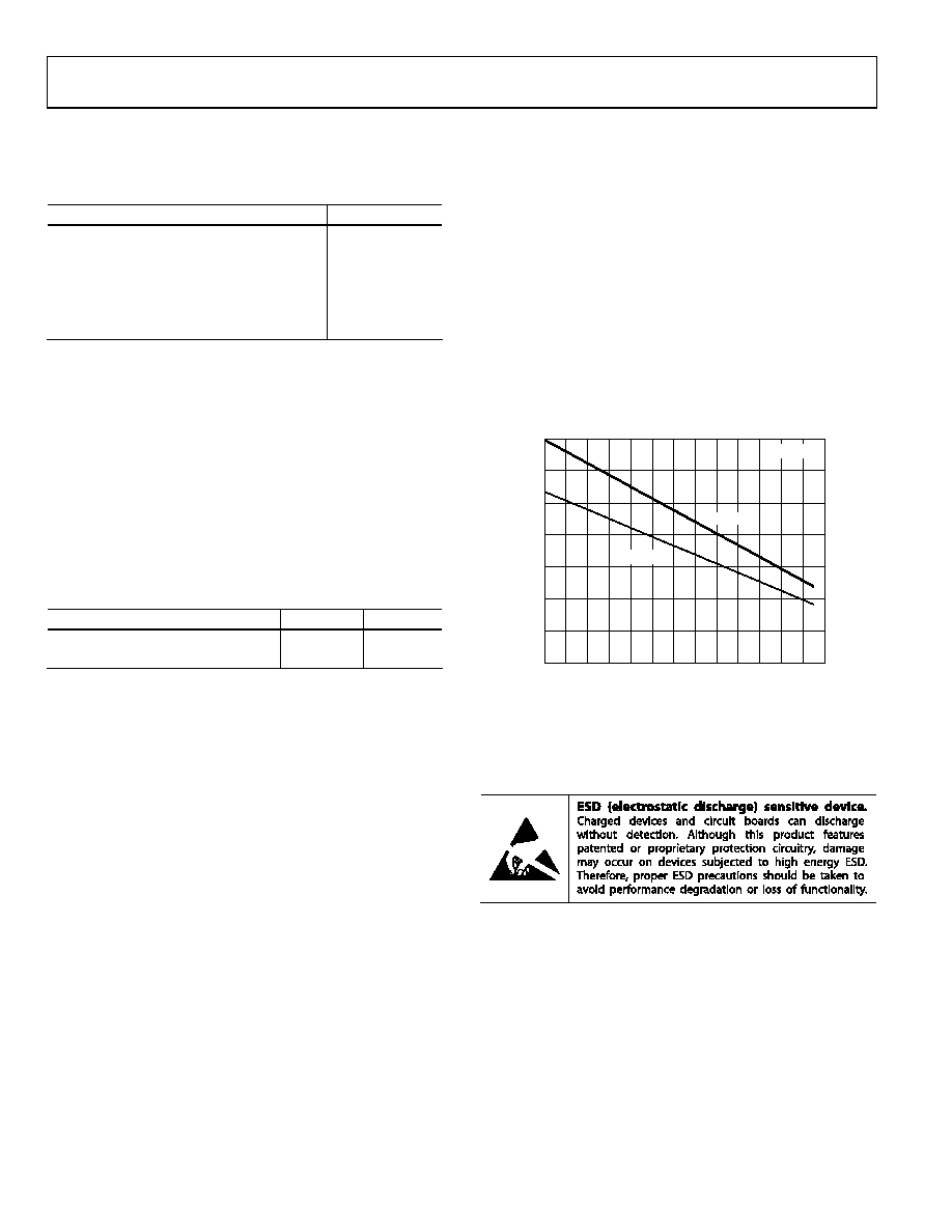
Figure 3 shows the maximum safe power dissipation in the
package vs. the ambient temperature for the LFCSP-32 and
TSSOP-28/EP packages on a JEDEC standard 4-layer board.
θJA values are approximations.
0
1
2
3
4
5
6
7
–40 –30 –20 –10
0
10
20
30
40
50
60
70
80
90
TEMPERATURE (°C)
M
AX
IM
U
M
P
O
W
E
R
DI
S
IP
AT
IO
N
(
W
)
TJ = 150°C
LFCSP-32
TSSOP-28/EP
0
64
77
-00
3
Figure 3. Maximum Power Dissipation vs. Temperature for a 4-Layer Board
See the Thermal Considerations section for additional thermal
design guidance.
ESD CAUTION
相关PDF资料 |
PDF描述 |
|---|---|
| AD8394AREZ-R7 | IC OPAMP ADSL/ADSL2 DL 20TSSOP |
| AD8396ACPZ-RL | IC LINE DRVR ADSL/ADSL2 16LFCSP |
| AD8398ACPZ-R7 | IC LINE DRVR DUAL VDSL 16-LFCSP |
| AD8403ARU1-REEL | IC POT DIG QUAD 1K 8BIT 24TSSOP |
| AD8494CRMZ | THERMOCOUPLE AMPLIFIER I |
相关代理商/技术参数 |
参数描述 |
|---|---|
| AD8392AAREZ-R7 | 功能描述:IC LINE DRVR ADSL/ADSL 28-TSSOP RoHS:是 类别:集成电路 (IC) >> 接口 - 驱动器,接收器,收发器 系列:- 标准包装:27 系列:- 类型:收发器 驱动器/接收器数:3/3 规程:RS232,RS485 电源电压:4.75 V ~ 5.25 V 安装类型:表面贴装 封装/外壳:28-SOIC(0.295",7.50mm 宽) 供应商设备封装:28-SOIC 包装:管件 |
| AD8392AAREZ-RL | 功能描述:IC LINE DRVR ADSL/ADSL 28-TSSOP RoHS:是 类别:集成电路 (IC) >> 接口 - 驱动器,接收器,收发器 系列:- 标准包装:121 系列:- 类型:收发器 驱动器/接收器数:1/1 规程:RS422,RS485 电源电压:3 V ~ 3.6 V 安装类型:表面贴装 封装/外壳:10-WFDFN 裸露焊盘 供应商设备封装:10-DFN(3x3) 包装:管件 |
| AD8392ACP-R2 | 制造商:Analog Devices 功能描述: 制造商:Rochester Electronics LLC 功能描述: |
| AD8392ACP-REEL | 制造商:Analog Devices 功能描述: |
| AD8392ACP-REEL7 | 制造商:Analog Devices 功能描述: 制造商:Rochester Electronics LLC 功能描述: |
发布紧急采购,3分钟左右您将得到回复。