- 您现在的位置:买卖IC网 > PDF目录1893 > AD8396ACPZ-RL (Analog Devices Inc)IC LINE DRVR ADSL/ADSL2 16LFCSP PDF资料下载
参数资料
| 型号: | AD8396ACPZ-RL |
| 厂商: | Analog Devices Inc |
| 文件页数: | 12/12页 |
| 文件大小: | 0K |
| 描述: | IC LINE DRVR ADSL/ADSL2 16LFCSP |
| 产品变化通告: | AD8396 Package Change 11/Sept/2009 AD8396 Discontinuation 17/Apr/2012 |
| 标准包装: | 5,000 |
| 类型: | 线路驱动器,发射器 |
| 驱动器/接收器数: | 2/0 |
| 电源电压: | 6 V ~ 24 V |
| 安装类型: | 表面贴装 |
| 封装/外壳: | 16-WQFN 裸露焊盘,CSP |
| 供应商设备封装: | 16-LFCSP-WQ(4x4) |
| 包装: | 带卷 (TR) |
AD8396
Rev. C | Page 9 of 12
APPLICATIONS INFORMATION
SUPPLIES, GROUNDING, AND LAYOUT
The AD8396 can be powered from either single or dual supplies,
with the total supply voltage ranging from 12 V to 24 V. For
optimum performance, use well-regulated low ripple supplies.
As with all high speed amplifiers, pay close attention to supply
decoupling, grounding, and overall board layout. Provide low
frequency supply decoupling with 10 μF tantalum capacitors
from each supply to ground. In addition, decouple all supply
pins with 0.1 μF quality ceramic chip capacitors placed as close
as possible to the driver. Use an internal low impedance ground
plane to provide a common ground point for all driver and
decoupling capacitor ground requirements. Whenever possible,
use separate ground planes for analog and digital circuitry.
Follow high speed layout techniques to minimize parasitic
capacitance.
Keep input and output traces as short as possible and as far
apart from each other as practical to minimize crosstalk. Keep
all differential signal traces as symmetrical as possible.
POWER MANAGEMENT
A digitally programmable logic pin switches each port of the
AD8396 between active bias and shutdown states. The PD_A
pin controls Port A and the PD_B pin controls Port B. These
pins can be controlled directly with either 3.3 V or 5 V CMOS
logic with the DGND pins as a reference. If left unconnected,
the PD pins float high, placing the amplifier in the shutdown
state. See the Specifications section for the quiescent current for
each of the available bias states.
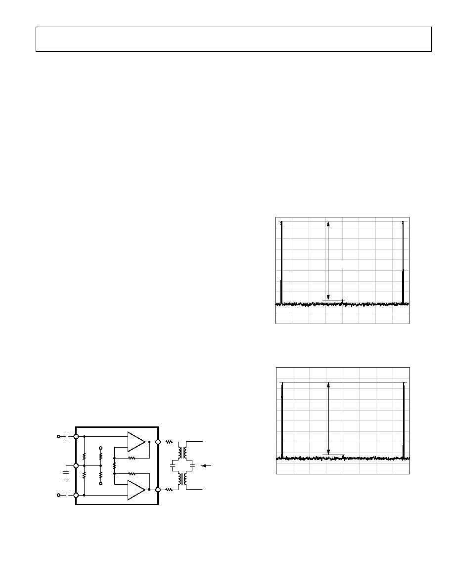
TYPICAL ADSL/ADSL2+ APPLICATION
In a typical ADSL/ADSL2+ application, a differential line driver
takes the signal from the analog front end (AFE) and drives it
onto the twisted pair telephone line. Referring to the typical
circuit representation in Figure 14, the differential input appears
at VIN+ and VIN from the AFE, while the differential output is
transformer coupled to the telephone line at TIP and RING.
The common-mode operating point, generally midway between
the supplies, is set internally and
is available at VCOM.
VCC
4k
VEE
+
–
VCOM
0.1F
+
VIN+
VIN–
1:N
TIP
RING
ROUT
Rm
07
02
2-
01
4
Figure 14. Typical ADSL/ADSL2+ Application Circuit
MULTITONE POWER RATIO (MTPR)
The DMT signal used in ADSL/ADSL2+ systems carries data in
discrete tones or bins, which appear in the frequency domain in
evenly spaced 4.3125 kHz intervals. In applications using this type
of waveform, MTPR is a commonly used measure of linearity.
Generally, designers are concerned with two types of MTPR:
in-band and out-of-band. In-band MTPR is defined as the
measured difference from the peak of one tone that is loaded
with data to the peak of an adjacent tone that is intentionally
left empty. Out-of-band MTPR is more loosely defined as the
spurious emissions that occur in the receive band located between
25.875 kHz and the first downstream tone at 138 kHz. Figure 15
and Figure 16 show the AD8396 in-band MTPR for a 5.5 crest
factor waveform for empty bins in the ADSL and extended
ADSL2+ bandwidths.
0
–100
642.131
651.619
FREQUENCY (kHz)
M
A
G
N
IT
UDE
(
d
Bm)
–20
–10
–30
–50
–70
–90
–40
–60
–80
644.503
646.875
649.247
–73dBc
07
02
2-
0
15
Figure 15. In-Band MTPR at 646.875 kHz
1.9618
1.9712
FREQUENCY (MHz)
M
A
G
N
IT
UDE
(
d
Bm)
1.9641
1.9665
1.9689
–68dBc
07
02
2-
0
16
0
–100
–20
–10
–30
–50
–70
–90
–40
–60
–80
Figure 16. In-Band MTPR at 1.9665 MHz
OBSOLETE
相关PDF资料 |
PDF描述 |
|---|---|
| AD8398ACPZ-R7 | IC LINE DRVR DUAL VDSL 16-LFCSP |
| AD8403ARU1-REEL | IC POT DIG QUAD 1K 8BIT 24TSSOP |
| AD8494CRMZ | THERMOCOUPLE AMPLIFIER I |
| AD8842ANZ | IC DAC 8BIT OCTAL 24DIP |
| AD9146BCPZRL | IC DAC 16BIT SRL DUAL 48LFCSP |
相关代理商/技术参数 |
参数描述 |
|---|---|
| AD8397 | 制造商:AD 制造商全称:Analog Devices 功能描述:Rail-to-Rail, High Output Current Amplifier |
| AD8397ARD-EBZ | 功能描述:BOARD EVAL FOR AD8397ARD RoHS:是 类别:编程器,开发系统 >> 评估板 - 运算放大器 系列:- 产品培训模块:Lead (SnPb) Finish for COTS Obsolescence Mitigation Program 标准包装:1 系列:- |
| AD8397ARDZ | 功能描述:IC OPAMP VF R-R DUAL LN 8SOIC RoHS:是 类别:集成电路 (IC) >> Linear - Amplifiers - Instrumentation 系列:- 标准包装:2,500 系列:- 放大器类型:通用 电路数:4 输出类型:- 转换速率:0.6 V/µs 增益带宽积:1MHz -3db带宽:- 电流 - 输入偏压:45nA 电压 - 输入偏移:2000µV 电流 - 电源:1.4mA 电流 - 输出 / 通道:40mA 电压 - 电源,单路/双路(±):3 V ~ 32 V,±1.5 V ~ 16 V 工作温度:0°C ~ 70°C 安装类型:表面贴装 封装/外壳:14-TSSOP(0.173",4.40mm 宽) 供应商设备封装:14-TSSOP 包装:带卷 (TR) 其它名称:LM324ADTBR2G-NDLM324ADTBR2GOSTR |
| AD8397ARDZ-REEL | 功能描述:IC OPAMP VF R-R DUAL LN 8SOIC RoHS:是 类别:集成电路 (IC) >> Linear - Amplifiers - Instrumentation 系列:- 产品培训模块:Lead (SnPb) Finish for COTS Obsolescence Mitigation Program 标准包装:1 系列:- 放大器类型:电流检测 电路数:1 输出类型:- 转换速率:- 增益带宽积:125kHz -3db带宽:- 电流 - 输入偏压:- 电压 - 输入偏移:100µV 电流 - 电源:1.1µA 电流 - 输出 / 通道:- 电压 - 电源,单路/双路(±):- 工作温度:-40°C ~ 85°C 安装类型:表面贴装 封装/外壳:4-WFBGA,CSPBGA 供应商设备封装:4-UCSP(2x2) 包装:剪切带 (CT) 其它名称:MAX9634WERS+TCT |
| AD8397ARDZREEL7 | 制造商:ANALOG 功能描述:NEW |
发布紧急采购,3分钟左右您将得到回复。