- 您现在的位置:买卖IC网 > PDF目录9301 > AD8400ARZ1-REEL (Analog Devices Inc)IC POT DGTL 8BIT SGL 1K 8SOIC PDF资料下载
参数资料
| 型号: | AD8400ARZ1-REEL |
| 厂商: | Analog Devices Inc |
| 文件页数: | 15/32页 |
| 文件大小: | 0K |
| 描述: | IC POT DGTL 8BIT SGL 1K 8SOIC |
| 标准包装: | 2,500 |
| 接片: | 256 |
| 电阻(欧姆): | 1k |
| 电路数: | 1 |
| 温度系数: | 标准值 500 ppm/°C |
| 存储器类型: | 易失 |
| 接口: | 3 线 SPI(芯片选择) |
| 电源电压: | 2.7 V ~ 5.5 V |
| 工作温度: | -40°C ~ 125°C |
| 安装类型: | 表面贴装 |
| 封装/外壳: | 8-SOIC(0.154",3.90mm 宽) |
| 供应商设备封装: | 8-SO |
| 包装: | 带卷 (TR) |
第1页第2页第3页第4页第5页第6页第7页第8页第9页第10页第11页第12页第13页第14页当前第15页第16页第17页第18页第19页第20页第21页第22页第23页第24页第25页第26页第27页第28页第29页第30页第31页第32页
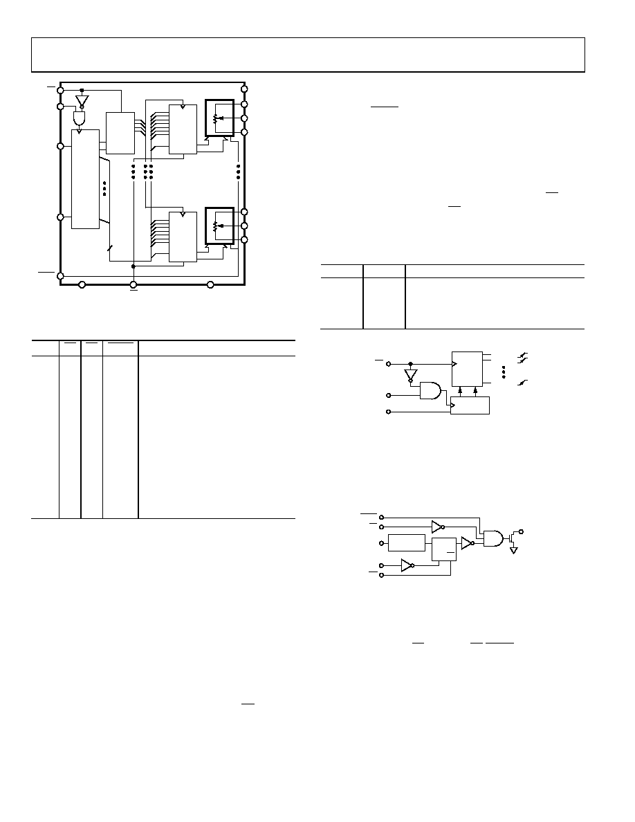
AD8400/AD8402/AD8403
Rev. E | Page 22 of 32
RDAC
LATCH
NO. 1
R
AGND
RS
A1
W1
B1
VDD
AD8403
CS
CLK
SDO
D7
D0
RDAC
LATCH
NO. 4
R
A4
W4
B4
D7
D0
EN
ADDR
DEC
A1
A0
D7
SDI
DO
DI
SER
REG
D0
SHDN
DGND
8
01
09
2-
0
47
Figure 48. AD8403 Block Diagram
Table 12. Input Logic Control Truth Table1
CLK
CS
RS
SHDN
Register Activity
L
H
No SR effect; enables SDO pin
P
L
H
Shift one bit in from the SDI pin. The
10th previously entered bit is shifted
out of the SDO pin.
X
P
H
Load SR data into RDAC latch based
on A1, A0 decode (Table 13).
X
H
No operation
X
L
H
Sets all RDAC latches to midscale,
wiper centered, and SDO latch
cleared
X
H
P
H
Latches all RDAC latches to 80H
X
H
L
Open-circuits all Resistor A terminals,
connects W to B, turns off SDO
output transistor.
1 P = positive edge, X = don’t care, SR = shift register
The serial data output (SDO) pin, which exists only on the
AD8403 and not on the AD8400 or AD8402, contains an
open-drain, n-channel FET that requires a pull-up resistor to
transfer data to the SDI pin of the next package. The pull-up
resistor termination voltage may be larger than the VDD supply
(but less than the max VDD of 8 V) of the AD8403 SDO output
device. For example, the AD8403 could operate at VDD = 3.3 V,
and the pull-up for interface to the next device could be set at 5 V.
This allows for daisy-chaining several RDACs from a single proc-
essor serial data line. The clock period needs to be increased
when using a pull-up resistor to the SDI pin of the following
device in the series. Capacitive loading at the daisy-chain node
SDO to SDI between devices must be accounted for in order to
transfer data successfully. When daisy chain is used, CS should
be kept low until all the bits of every package are clocked into
their respective serial registers and the address and data bits are
in the proper decoding location.
If two AD8403 RDACs are daisy-chained, it requires 20 bits
of address and data in the format shown in Table 6. During
shutdown (SHDN = logic low), the SDO output pin is forced
to the off (logic high) state to disable power dissipation in the
pull-up resistor. See
for equivalent SDO output circuit
schematic.
The data setup and hold times in the specification table deter-
mine the data valid time requirements. The last 10 bits of the
data-word entered into the serial register are held when CS
returns high. At the same time CS goes high it gates the address
decoder, which enables one of the two (AD8402) or four (AD8403)
positive edge-triggered RDAC latches. See
and
.
Table 13. Address Decode Table
A1
A0
Latch Decoded
0
RDAC#1
0
1
RDAC#2
1
0
RDAC#3 AD8403 Only
1
RDAC#4 AD8403 Only
ADDR
DECODE
RDAC 1
RDAC 2
RDAC 4
SERIAL
REGISTER
AD8403
SDI
CLK
CS
0
10
92
-04
8
Figure 49. Equivalent Input Control Logic
The target RDAC latch is loaded with the last eight bits of the
serial data-word completing one RDAC update. In the case of
AD8403, four separate 10-bit data-words must be clocked in to
change all four VR settings.
SERIAL
REGISTER
SDI
CK RS
D
SHDN
CS
CLK
RS
SDO
0
10
92
-0
49
Q
Figure 50. Detailed SDO Output Schematic of the AD8403
All digital pins are protected with a series input resistor and
parallel Zener ESD structure shown in Figure 51. This structure
applies to digital pins CS, SDI, SDO, RS, SHDN, and CLK. The
digital input ESD protection allows for mixed power supply
applications where 5 V CMOS logic can be used to drive an
AD8400, AD8402, or AD8403 operating from a 3 V power
supply. Analog Pin A, Pin B, and Pin W are protected with a
20 Ω series resistor and parallel Zener diode (see
).
相关PDF资料 |
PDF描述 |
|---|---|
| MS27508E22A21SA | CONN RCPT 21POS BOX MNT W/SCKT |
| MS27474T24F35P | CONN RCPT 128POS JAM NUT W/PINS |
| MS27466P23A35SA | CONN RCPT 100POS WALL MNT W/SCKT |
| AD8400ARZ50-REEL | IC POT DGTL 8BIT 50K 1CH 8SOIC |
| GTC06CF-20-2P | CONN PLUG 1POS STRAIGHT W/PINS |
相关代理商/技术参数 |
参数描述 |
|---|---|
| AD8400ARZ50 | 功能描述:IC POT DGTL 8BIT SGL 50K 8-SOIC RoHS:是 类别:集成电路 (IC) >> 数据采集 - 数字电位器 系列:- 产品培训模块:Lead (SnPb) Finish for COTS Obsolescence Mitigation Program 标准包装:1 系列:- 接片:256 电阻(欧姆):100k 电路数:1 温度系数:标准值 35 ppm/°C 存储器类型:非易失 接口:3 线串口 电源电压:2.7 V ~ 5.25 V 工作温度:-40°C ~ 85°C 安装类型:表面贴装 封装/外壳:8-WDFN 裸露焊盘 供应商设备封装:8-TDFN-EP(3x3) 包装:剪切带 (CT) 产品目录页面:1399 (CN2011-ZH PDF) 其它名称:MAX5423ETA+TCT |
| AD8400ARZ50-REEL | 功能描述:IC POT DGTL 8BIT 50K 1CH 8SOIC RoHS:是 类别:集成电路 (IC) >> 数据采集 - 数字电位器 系列:- 标准包装:3,000 系列:DPP 接片:32 电阻(欧姆):10k 电路数:1 温度系数:标准值 300 ppm/°C 存储器类型:非易失 接口:3 线串行(芯片选择,递增,增/减) 电源电压:2.5 V ~ 6 V 工作温度:-40°C ~ 85°C 安装类型:表面贴装 封装/外壳:8-WFDFN 裸露焊盘 供应商设备封装:8-TDFN(2x3) 包装:带卷 (TR) |
| AD8401 | 制造商:AD 制造商全称:Analog Devices 功能描述:8-Bit, 4-Channel Data Acquisition System |
| AD8401AR | 制造商:Rochester Electronics LLC 功能描述:8-BIT,4-CHANNEL A/D CONV - Bulk 制造商:Analog Devices 功能描述: |
| AD8401ARZ | 制造商:Analog Devices 功能描述:DATA ACQ SYS SGL ADC SGL DAC 8BIT 28SOIC - Rail/Tube |
发布紧急采购,3分钟左右您将得到回复。