参数资料
| 型号: | AD8420ARMZ-R7 |
| 厂商: | Analog Devices Inc |
| 文件页数: | 13/28页 |
| 文件大小: | 0K |
| 描述: | IC AMP INSTR RR 2.5KHZ 8MSOP |
| 标准包装: | 1,000 |
| 放大器类型: | 仪表 |
| 电路数: | 1 |
| 输出类型: | 满摆幅 |
| 转换速率: | 1 V/µs |
| -3db带宽: | 250kHz |
| 电流 - 输入偏压: | 20nA |
| 电压 - 输入偏移: | 250µV |
| 电流 - 电源: | 85µA |
| 电流 - 输出 / 通道: | 10mA |
| 电压 - 电源,单路/双路(±): | 2.7 V ~ 36 V,±2.7 V ~ 18 V |
| 工作温度: | -40°C ~ 85°C |
| 安装类型: | 表面贴装 |
| 封装/外壳: | 8-TSSOP,8-MSOP(0.118",3.00mm 宽) |
| 供应商设备封装: | 8-MSOP |
| 包装: | 带卷 (TR) |
第1页第2页第3页第4页第5页第6页第7页第8页第9页第10页第11页第12页当前第13页第14页第15页第16页第17页第18页第19页第20页第21页第22页第23页第24页第25页第26页第27页第28页
AD8420
Data Sheet
Rev. 0 | Page 20 of 28
GAIN ACCURACY
Unlike most instrumentation amplifiers, the relative match of
the two gain setting resistors determines the gain accuracy of
the AD8420 rather than a single resistor. For example, if two
resistors have exactly the same absolute error, there is no error
in gain. Conversely, two 1% resistors can cause approximately 2%
maximum gain error at high gains. Temperature coefficient
mismatch of the gain setting resistors increases the gain drift
of the instrumentation amplifier circuit. Because these external
resistors do not have to match any on-chip resistors, resistors
with good TC tracking can achieve excellent gain drift.
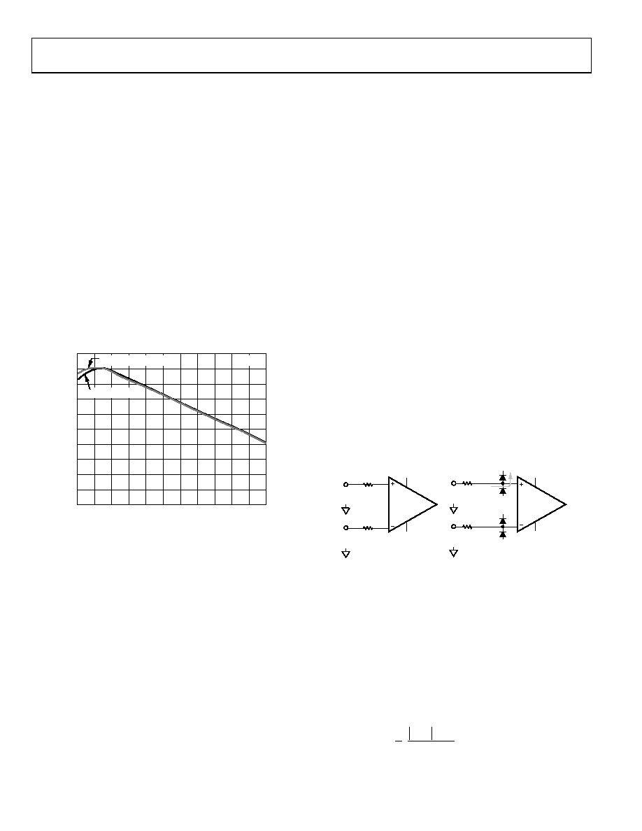
When the differential voltage at the inputs approaches the
differential input limit, the diodes start to conduct, limiting
the voltage seen by the inputs. This can look like increased gain
error at large differential inputs. Performance of the AD8420 is
specified for ±1 V differential from 40°C to +85°C.However,
at higher temperatures, the reduced forward voltage of the diodes
limits the differential input to a smaller voltage. Figure 60 tracks
1% error across the operating temperature range to show the
effect of temperature on the input limit.
–40 –25 –10
5
20
35
50
65
80
95
110 125
MA
XI
MU
M
I
N
PU
T
VO
LT
A
G
E
(1
%
E
R
O
R
)
TEMPERATURE (°C)
099
45-
5
03
0
2.0
1.8
1.6
1.4
1.2
1.0
0.8
0.6
0.4
0.2
POSITIVE VOLTAGE
NEGATIVE VOLTAGE
VS = ±15V
Figure 60. Differential Input Limit vs. Temperature
INPUT VOLTAGE RANGE
The allowed input range of the AD8420 is much simpler than
traditional architectures. For the transfer function of the AD8420
to be valid, the input voltage should follow two rules:
Keep the differential input voltage within ±1 V.
Keep the voltage on the +IN, IN, REF, and FB pins in the
specified input voltage range.
Because the output swing is completely independent of the
input common-mode voltage, there are no hexagonal figures
or complicated formulas to follow, and no limitation for the
output swing the amplifier has for input signals with changing
common mode.
INPUT PROTECTION
The current into the AD8420 inputs is limited internally. This
ensures that the diodes that limit the differential voltage seen by
the internal amplifier do not draw excessive current when they
turn on. The part can handle large differential input voltages,
regardless of the amount of gain applied, without damage. As a
result, the AD8420 inputs are protected from voltages beyond
the positive rail. If voltages beyond the negative rail are expected,
external protection must be used.
Keep all of the AD8420 terminals within the voltage range specified
in the Absolute Maximum Ratings section. All terminals of the
AD8420 are protected against ESD.
Input Voltages Beyond the Rails
For applications that require protection beyond the negative rail,
one option is to use an external resistor in series with each input
to limit current during overload conditions. In this case, size the
resistors to limit the current into the AD8420 to 6 mA.
RPROTECT ≥ (Negative Supply VIN)/6 mA
40 V limitation, the I × R drop across the protection resistor
increases the protection on the positive side to approximately
(40 V + Negative Supply) + 300 μA × RPROTECT
An alternate protection method is to place diodes at the AD8420
inputs to limit voltage and resistors in series with the inputs to
limit the current into these diodes. To keep input bias current at
a minimum for normal operation, use low leakage diode clamps,
such as the BAV199. The AD8420 also combines well with TVS
diodes, such as the PTVSxS1UR.
SIMPLE METHOD
ALTERNATE METHOD
AD8420
RPROTECT
VIN+
+
–
VIN–
VIN+
VIN–
+
–
+VS
AD8420
–VS
+VS
–VS
+VS
–VS
+VS
–VS
I
+
–
+
–
09
94
5
-16
0
Figure 61. Protection for Voltages Beyond the Rails
Large Differential Input Voltage
The AD8420 is able to handle large differential input voltage
Figure 11, and Figure 12 for overvoltage performance. The
AD8420 differential voltage is internally limited with diodes to
±1 V. If this limit is exceeded, the diodes start to conduct and
draw current, as shown in Figure 22. This current is limited
internally to a value that is safe for the AD8420, but if the input
current cannot be tolerated in the system, place resistors in
series with each input with the following value:
≥
MAX
DIFF
PROTECT
I
V
R
V
1
2
1
相关PDF资料 |
PDF描述 |
|---|---|
| AD8421BRMZ | IC OP AMP INSTRUMENTATION 8MSOP |
| AD8426ACPZ-R7 | IC AMP INSTR RR 1.5MHZ 16LFCSP |
| AD8428BRZ | IC OPAMP INST 3.5MHZ LN 8SOIC |
| AD8429BRZ-R7 | IC OP AMP INST LOW NOISE 8SOIC |
| AD842JQ | IC OPAMP GP 80MHZ 100MA 14CDIP |
相关代理商/技术参数 |
参数描述 |
|---|---|
| AD8420ARMZ-RL | 功能描述:IC AMP INSTR RR 2.5KHZ 8MSOP RoHS:是 类别:集成电路 (IC) >> Linear - Amplifiers - Instrumentation 系列:- 标准包装:2,500 系列:- 放大器类型:通用 电路数:1 输出类型:满摆幅 转换速率:0.11 V/µs 增益带宽积:350kHz -3db带宽:- 电流 - 输入偏压:4nA 电压 - 输入偏移:20µV 电流 - 电源:260µA 电流 - 输出 / 通道:20mA 电压 - 电源,单路/双路(±):2.7 V ~ 36 V,±1.35 V ~ 18 V 工作温度:-40°C ~ 85°C 安装类型:表面贴装 封装/外壳:8-SOIC(0.154",3.90mm 宽) 供应商设备封装:8-SO 包装:带卷 (TR) |
| AD8420BRMZ | 制造商:AD 制造商全称:Analog Devices 功能描述:Wide Supply Range, Rail-to-Rail Output Instrumentation Amplifier |
| AD8420BRMZ-R7 | 制造商:AD 制造商全称:Analog Devices 功能描述:Wide Supply Range, Rail-to-Rail Output Instrumentation Amplifier |
| AD8420BRMZ-RL | 制造商:AD 制造商全称:Analog Devices 功能描述:Wide Supply Range, Rail-to-Rail Output Instrumentation Amplifier |
| AD8421 | 制造商:AD 制造商全称:Analog Devices 功能描述:3 nV/√Hz, Low Power |
发布紧急采购,3分钟左右您将得到回复。