参数资料
| 型号: | AD8426ACPZ-R7 |
| 厂商: | Analog Devices Inc |
| 文件页数: | 14/28页 |
| 文件大小: | 0K |
| 描述: | IC AMP INSTR RR 1.5MHZ 16LFCSP |
| 标准包装: | 1 |
| 放大器类型: | 仪表 |
| 电路数: | 2 |
| 输出类型: | 满摆幅 |
| 转换速率: | 0.6 V/µs |
| -3db带宽: | 1MHz |
| 电流 - 输入偏压: | 20nA |
| 电压 - 输入偏移: | 200µV |
| 电流 - 电源: | 350µA |
| 电流 - 输出 / 通道: | 13mA |
| 电压 - 电源,单路/双路(±): | 2.2 V ~ 36 V,±1.35 V ~ 18 V |
| 工作温度: | -40°C ~ 125°C |
| 安装类型: | 表面贴装 |
| 封装/外壳: | 16-VQFN,CSP |
| 供应商设备封装: | 16-LFCSP(4x4) |
| 包装: | 标准包装 |
| 其它名称: | AD8426ACPZ-R7DKR |
第1页第2页第3页第4页第5页第6页第7页第8页第9页第10页第11页第12页第13页当前第14页第15页第16页第17页第18页第19页第20页第21页第22页第23页第24页第25页第26页第27页第28页
AD8426
Rev. 0 | Page 21 of 28
THEORY OF OPERATION
A3
R2
24.7k
R1
24.7k
A1
A2
Q2
Q1
–IN
+IN
+VS
–VS
R3
50k
R4
50k
R5
50k
RB
+VS
–VS
VOUT
REF
NODE 1
NODE 2
RG
VBIAS
+VS
–VS
+VS
–VS
NODE 4
NODE 3
R6
50k
DIFFERENCE
AMPLIFIER STAGE
GAIN STAGE
ESD AND
OVERVOLTAGE
PROTECTION
ESD AND
OVERVOLTAGE
PROTECTION
–VS
0
94
90
-0
03
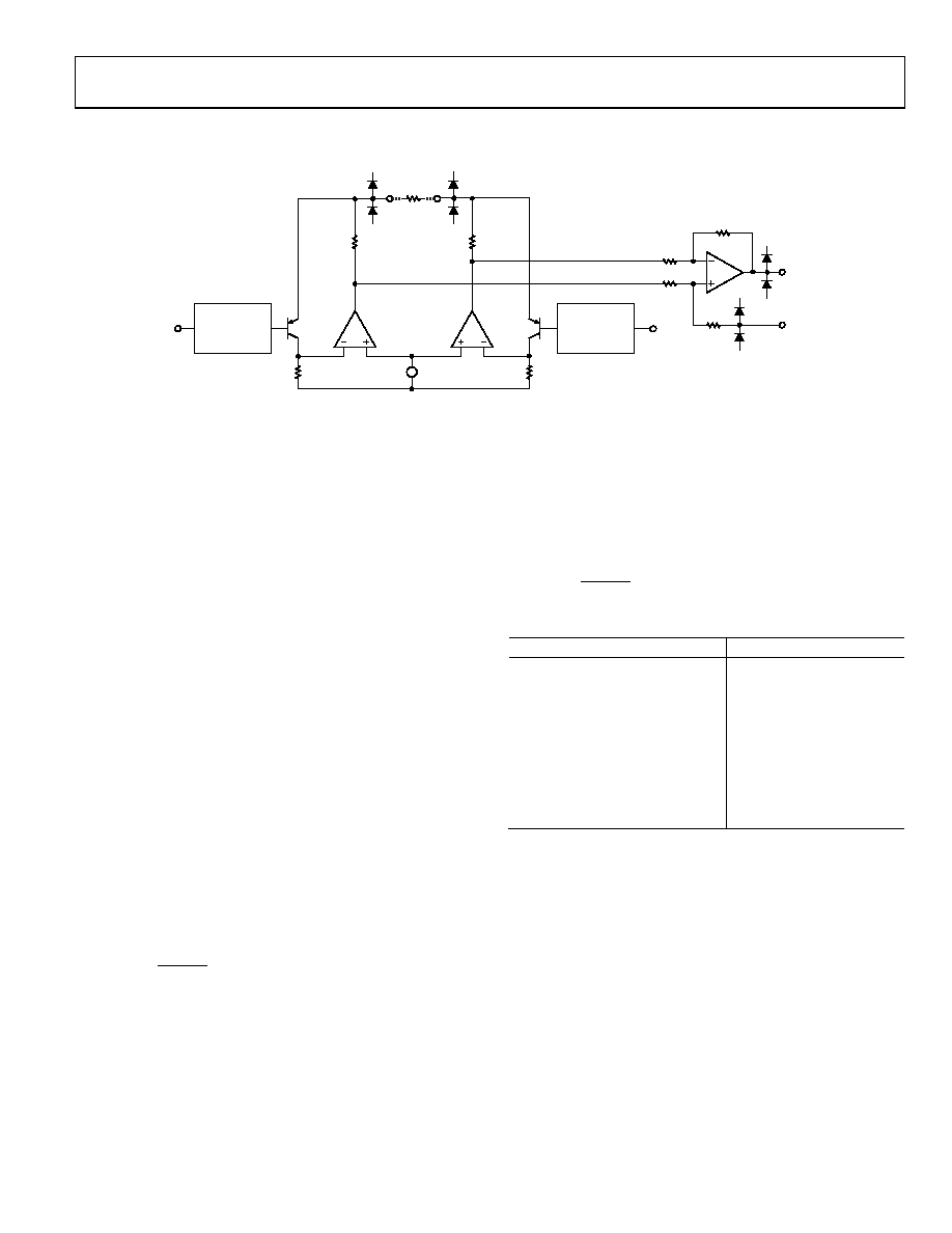
Figure 61. Simplified Schematic
ARCHITECTURE
The AD8426 is based on the classic 3-op-amp topology. This
topology has two stages: a gain stage (preamplifier) to provide
differential amplification, followed by a difference amplifier stage
to remove the common-mode voltage. Figure 61 shows a simplified
schematic of one of the instrumentation amplifiers in the AD8426.
The first stage works as follows. To maintain a constant voltage
across the bias resistor, RB, A1 must keep Node 3 at a constant
diode drop above the positive input voltage. Similarly, A2 keeps
Node 4 at a constant diode drop above the negative input voltage.
Therefore, a replica of the differential input voltage is placed
across the gain setting resistor, RG. The current that flows across
this resistance must also flow through the R1 and R2 resistors,
creating a gained differential signal between the A2 and A1 out-
puts. Note that, in addition to a gained differential signal, the
original common-mode signal, shifted up by a diode drop, is
also still present.
The second stage is a difference amplifier, composed of A3 and
four 50 kΩ resistors. The purpose of this stage is to remove the
common-mode signal from the amplified differential signal.
The transfer function of the AD8426 is
VOUT = G × (VIN+ VIN) + VREF
where:
G
R
G
kΩ
49.4
1 +
=
GAIN SELECTION
Placing a resistor across the RG terminals sets the gain of the
or by using the following gain equation:
1
kΩ
49.4
=
G
R
G
Table 11. Gains Achieved Using 1% Resistors
1% Standard Table Value of RG
Calculated Gain
49.9 kΩ
1.990
12.4 kΩ
4.984
5.49 kΩ
9.998
2.61 kΩ
19.93
1.00 kΩ
50.40
499 Ω
100.0
249 Ω
199.4
100 Ω
495.0
49.9 Ω
991.0
The AD8426 defaults to G = 1 when no gain resistor is used.
The tolerance and gain drift of the RG resistor should be added
to the AD8426 specifications to determine the total gain accu-
racy of the system. When the gain resistor is not used, gain
error and gain drift are minimal.
相关PDF资料 |
PDF描述 |
|---|---|
| AD8428BRZ | IC OPAMP INST 3.5MHZ LN 8SOIC |
| AD8429BRZ-R7 | IC OP AMP INST LOW NOISE 8SOIC |
| AD842JQ | IC OPAMP GP 80MHZ 100MA 14CDIP |
| AD8432ACPZ-R7 | IC OPAMP VF DUAL LN LP 24LFCSP |
| AD843SQ | IC OPAMP GP 34MHZ 50MA 8CDIP |
相关代理商/技术参数 |
参数描述 |
|---|---|
| AD8426ACPZ-R7_PROMO | 制造商:Analog Devices 功能描述:IC INSTR AMP 1MHZ 80DB LFC |
| AD8426ACPZ-WP | 功能描述:IC AMP INSTR RR 1.5MHZ 16LFCSP RoHS:是 类别:集成电路 (IC) >> Linear - Amplifiers - Instrumentation 系列:- 标准包装:2,500 系列:- 放大器类型:通用 电路数:4 输出类型:- 转换速率:0.6 V/µs 增益带宽积:1MHz -3db带宽:- 电流 - 输入偏压:45nA 电压 - 输入偏移:2000µV 电流 - 电源:1.4mA 电流 - 输出 / 通道:40mA 电压 - 电源,单路/双路(±):3 V ~ 32 V,±1.5 V ~ 16 V 工作温度:0°C ~ 70°C 安装类型:表面贴装 封装/外壳:14-TSSOP(0.173",4.40mm 宽) 供应商设备封装:14-TSSOP 包装:带卷 (TR) 其它名称:LM324ADTBR2G-NDLM324ADTBR2GOSTR |
| AD8426BCPZ-R7 | 功能描述:IC AMP INSTR RR 1.5MHZ 16LFCSP RoHS:是 类别:集成电路 (IC) >> Linear - Amplifiers - Instrumentation 系列:- 标准包装:73 系列:Over-The-Top® 放大器类型:通用 电路数:4 输出类型:满摆幅 转换速率:0.07 V/µs 增益带宽积:200kHz -3db带宽:- 电流 - 输入偏压:1nA 电压 - 输入偏移:285µV 电流 - 电源:50µA 电流 - 输出 / 通道:25mA 电压 - 电源,单路/双路(±):2 V ~ 44 V,±1 V ~ 22 V 工作温度:-40°C ~ 85°C 安装类型:表面贴装 封装/外壳:16-WFDFN 裸露焊盘 供应商设备封装:16-DFN-EP(5x3) 包装:管件 |
| AD8426BCPZ-R7_PROMO | 制造商:Analog Devices 功能描述:INSTR-AMPLIFIER 1MHZ 90DB L |
| AD8426BCPZ-WP | 功能描述:IC AMP INSTR RR 1.5MHZ 16LFCSP RoHS:是 类别:集成电路 (IC) >> Linear - Amplifiers - Instrumentation 系列:- 标准包装:150 系列:- 放大器类型:音频 电路数:2 输出类型:- 转换速率:5 V/µs 增益带宽积:12MHz -3db带宽:- 电流 - 输入偏压:100nA 电压 - 输入偏移:500µV 电流 - 电源:6mA 电流 - 输出 / 通道:50mA 电压 - 电源,单路/双路(±):4 V ~ 32 V,±2 V ~ 16 V 工作温度:-40°C ~ 85°C 安装类型:表面贴装 封装/外壳:8-TSSOP(0.173",4.40mm 宽) 供应商设备封装:8-TSSOP 包装:管件 |
发布紧急采购,3分钟左右您将得到回复。