参数资料
| 型号: | AD8428ARZ-RL |
| 厂商: | Analog Devices Inc |
| 文件页数: | 11/20页 |
| 文件大小: | 0K |
| 描述: | IC AMP INSTRUMENTATON 8SOIC |
| 标准包装: | 2,500 |
| 放大器类型: | 仪表 |
| 电路数: | 1 |
| 转换速率: | 50 V/µs |
| -3db带宽: | 3.5MHz |
| 电流 - 输入偏压: | 200nA |
| 电压 - 输入偏移: | 100µV |
| 电流 - 电源: | 6.5mA |
| 电流 - 输出 / 通道: | 30mA |
| 电压 - 电源,单路/双路(±): | ±4 V ~ 18 V |
| 工作温度: | -40°C ~ 85°C |
| 安装类型: | 表面贴装 |
| 封装/外壳: | 8-SOIC(0.154",3.90mm 宽) |
| 供应商设备封装: | 8-SO |
| 包装: | 带卷 (TR) |
Data Sheet
AD8428
Rev. A | Page 19 of 20
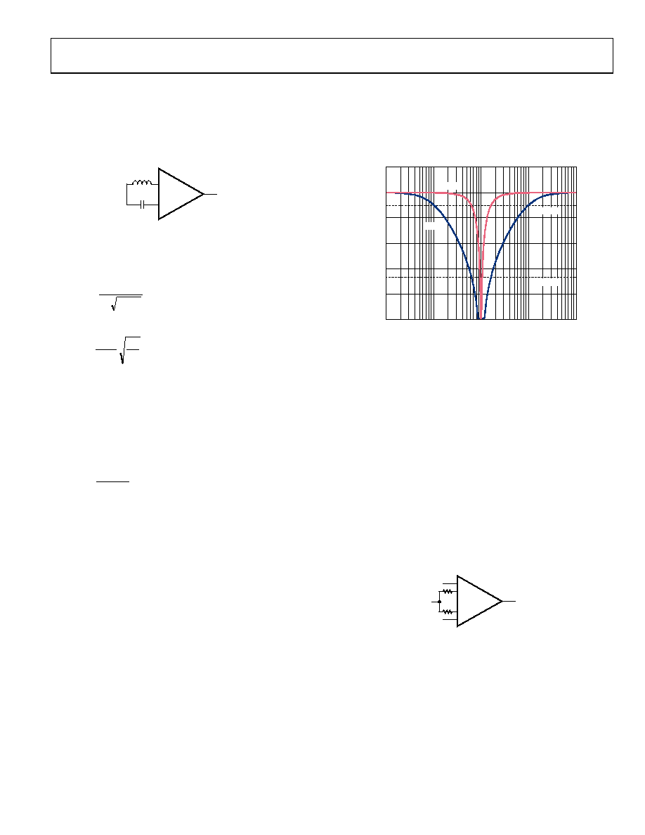
Notch Filter
In cases where the frequency of the interfering signal is well
known, a notch filter can be implemented to help minimize the
impact of the known signal on the measurement. The filter can
be realized by adding a series LC network between the filter
pins, as shown in Figure 48.
+
–
AD8428
OUT
CF
+FIL
–FIL
LF
0
973
1-
147
Figure 48. Notch Filter Example
The inductor and capacitor form a resonant circuit that rejects
frequencies near the notch. The center frequency can be
calculated using the following equation:
F
N
C
L
f
π
=
2
1
The Q factor of the filter is given by the following equation:
F
C
L
Q
6000
1
=
The accuracy of the center frequency, fN, depends only on the
tolerance of the capacitor and inductor values, not on the value
of the internal resistors. However, the Q of the circuit depends on
both the tolerance of the external components and the absolute
tolerance of the internal resistors, which is typically 10%.
The Q factor is a filter parameter that indicates how narrow the
notch filter is. It is defined as follows:
A
B
N
f
Q
=
where fA and fB are the frequencies at which there is 3 dB
attenuation on each side of the notch.
This equation indicates that the higher the Q, the narrower the
notch—that is, high values of Q increase the selectivity of the
notch. In other words, although high values of Q reduce the
effect of the notch on the amplitude and phase in neighboring
frequencies, the ability to reject the undesired frequency may
also be reduced due to mismatch between it and the actual
center frequency. This mismatch can be caused by frequency
variations on the affecting source and the tolerance of the filter
inductor and capacitor values.
In contrast, low values of Q work better to ensure that the
interfering frequency is attenuated, but these low values also
affect the signal of interest if it is located close to the center
frequency of the notch.
For example, if the goal is to attenuate the interfering signal by
20 dB, a large Q value reduces the frequency range where the
notch is effective, as shown in Figure 49.
In contrast, a small Q value increases the range for the same
attenuation, which relaxes the tolerance requirements between
the inductor and capacitor and the frequency uncertainty of the
undesired signal. However, the lower Q value has a significant
effect on signal bandwidth one decade before the notch
frequency.
72
66
60
54
36
0.01fN
0.1fN
fN
10fN
100fN
MA
G
N
IT
U
D
E
(
d
B
)
FREQUENCY (Hz)
48
42
Q = 0.1
Q = 1
09731
-249
–3dB
–20dB
Figure 49. Notch Filter Attenuation with Q = 0.1 and Q = 1
Around the Center Frequency
The maximum attenuation that can be achieved with a notch
filter is at its center frequency, fN. This maximum attenuation
(or depth of the notch) depends on the equivalent series
resistance of the inductor and capacitor at the center frequency.
Choosing components with high quality factors improves the
rejection at the filter’s center frequency. For information about
calculating the maximum allowed series resistance at the frequency
of interest to obtain the desired attenuation, see the Setting the
Amplifier to Different Gains section.
Extracting the Common-Mode Voltage of the Input
The common-mode signal present at the input terminals can be
extracted by inserting two resistors between the filter terminals
and tapping from the center, as shown in Figure 50. The common-
mode voltage, VCM, is the average of the voltages present at the
two inputs minus a 0.6 V drop.
+IN
–IN
+
–
AD8428
OUT
R
+FIL
–FIL
R
VCM
09
73
1
-14
8
Figure 50. Extracting the Common-Mode Voltage
Use resistor values that are high enough to minimize the impact
on gain accuracy. For example, resistor values of 2 MΩ introduce
an additional gain error of less than 0.2%. For information about
the impact of these resistors on the gain of the amplifier, see the
相关PDF资料 |
PDF描述 |
|---|---|
| 961242-6404-AR | CONN HEADER VERT DUAL 42POS GOLD |
| N3314-2303RB | CONN HEADER 14POS .100" STR GOLD |
| AD8224HACPZ-WP | IC AMP INST DUAL PREC LN 16LFCSP |
| AD797BR-REEL7 | IC OPAMP GP 110MHZ ULDIST 8SOIC |
| TSM-105-02-S-DV-P-TR | CONN HEADER 10POS .100" DBL SMD |
相关代理商/技术参数 |
参数描述 |
|---|---|
| AD8428BRZ | 功能描述:IC OPAMP INST 3.5MHZ LN 8SOIC RoHS:是 类别:集成电路 (IC) >> Linear - Amplifiers - Instrumentation 系列:- 标准包装:2,500 系列:Excalibur™ 放大器类型:J-FET 电路数:1 输出类型:- 转换速率:45 V/µs 增益带宽积:10MHz -3db带宽:- 电流 - 输入偏压:20pA 电压 - 输入偏移:490µV 电流 - 电源:1.7mA 电流 - 输出 / 通道:48mA 电压 - 电源,单路/双路(±):4.5 V ~ 38 V,±2.25 V ~ 19 V 工作温度:-40°C ~ 85°C 安装类型:表面贴装 封装/外壳:8-SOIC(0.154",3.90mm 宽) 供应商设备封装:8-SOIC 包装:带卷 (TR) |
| AD8428BRZ_PROMO | 制造商:Analog Devices 功能描述:INST AMP 3.5MHZ 2K V/V 0.2 |
| AD8428BRZ-RL | 功能描述:IC OPAMP INST 3.5MHZ LN 8SOIC RoHS:是 类别:集成电路 (IC) >> Linear - Amplifiers - Instrumentation 系列:- 标准包装:2,500 系列:Excalibur™ 放大器类型:J-FET 电路数:1 输出类型:- 转换速率:45 V/µs 增益带宽积:10MHz -3db带宽:- 电流 - 输入偏压:20pA 电压 - 输入偏移:490µV 电流 - 电源:1.7mA 电流 - 输出 / 通道:48mA 电压 - 电源,单路/双路(±):4.5 V ~ 38 V,±2.25 V ~ 19 V 工作温度:-40°C ~ 85°C 安装类型:表面贴装 封装/外壳:8-SOIC(0.154",3.90mm 宽) 供应商设备封装:8-SOIC 包装:带卷 (TR) |
| AD8429 | 制造商:AD 制造商全称:Analog Devices 功能描述:Low Noise, Low Gain Drift, G = 2000 |
| AD8429ARZ | 功能描述:IC OP AMP INST LOW NOISE 8SOIC RoHS:是 类别:集成电路 (IC) >> Linear - Amplifiers - Instrumentation 系列:- 标准包装:1 系列:- 放大器类型:通用 电路数:4 输出类型:满摆幅 转换速率:0.028 V/µs 增益带宽积:105kHz -3db带宽:- 电流 - 输入偏压:3nA 电压 - 输入偏移:100µV 电流 - 电源:3.3µA 电流 - 输出 / 通道:12mA 电压 - 电源,单路/双路(±):2.7 V ~ 12 V,±1.35 V ~ 6 V 工作温度:-40°C ~ 85°C 安装类型:表面贴装 封装/外壳:14-TSSOP(0.173",4.40mm 宽) 供应商设备封装:14-TSSOP 包装:剪切带 (CT) 其它名称:OP481GRUZ-REELCT |
发布紧急采购,3分钟左右您将得到回复。