参数资料
| 型号: | AD8432ACPZ-R7 |
| 厂商: | Analog Devices Inc |
| 文件页数: | 14/32页 |
| 文件大小: | 0K |
| 描述: | IC OPAMP VF DUAL LN LP 24LFCSP |
| 标准包装: | 1,500 |
| 放大器类型: | 电压反馈 |
| 电路数: | 2 |
| 输出类型: | 差分 |
| 转换速率: | 295 V/µs |
| -3db带宽: | 200MHz |
| 电压 - 输入偏移: | 1000µV |
| 电流 - 电源: | 24mA |
| 电流 - 输出 / 通道: | 77mA |
| 电压 - 电源,单路/双路(±): | 4.5 V ~ 5.5 V |
| 工作温度: | -40°C ~ 85°C |
| 安装类型: | 表面贴装 |
| 封装/外壳: | 24-WFQFN 裸露焊盘,CSP |
| 供应商设备封装: | 24-LFCSP-WQ(4x4) |
| 包装: | 带卷 (TR) |
第1页第2页第3页第4页第5页第6页第7页第8页第9页第10页第11页第12页第13页当前第14页第15页第16页第17页第18页第19页第20页第21页第22页第23页第24页第25页第26页第27页第28页第29页第30页第31页第32页
Data Sheet
AD8432
Rev. C | Page 21 of 32
APPLICATIONS INFORMATION
The AD8432 LNA provides precision gain and ultralow noise
performance with minimal external components. Because it is
a high performance part, care must be taken to ensure that it is
configured optimally to attain the best performance and dynamic
range for the system.
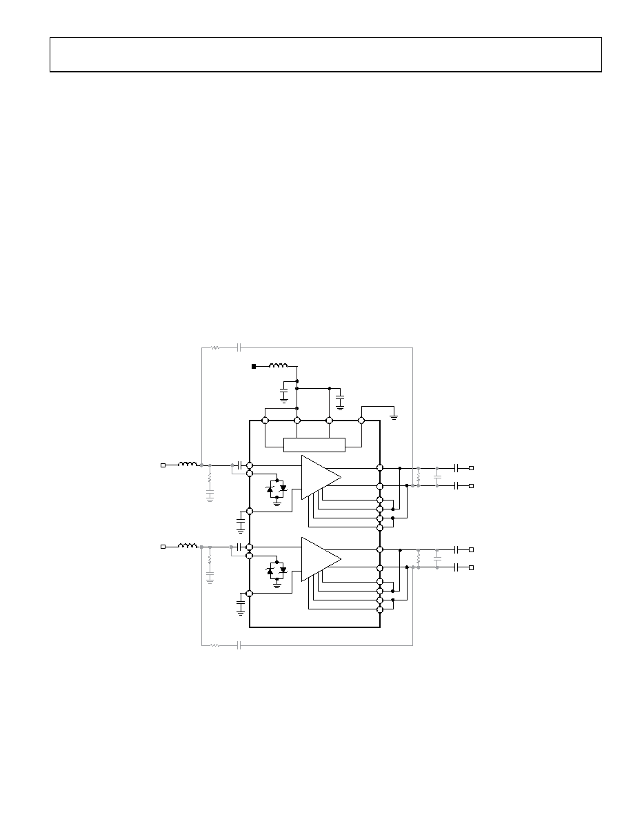
TYPICAL SETUP
The internal bias circuitry of the AD8432 sets the input bias
voltage at 3.25 V and the output bias voltage at 2.5 V. It is important
to ac couple the inputs through a capacitor to maintain the internal
dc bias levels. When active input termination is used (RFB), a
decoupling capacitor (CFB) is required to isolate the input and
output bias voltages of the LNA. A typical value for CFB is 0.1 F, but
a smaller value capacitor is more appropriate at higher frequencies.
The unterminated input impedance of the AD8432 is 6.2 kΩ.
Any input resistance between 50 Ω and 6.2 kΩ can be synthesized
using active impedance matching.
At the lowest gain (12.04 dB), the gain response exhibits some
peaking at higher frequencies. A resistor-capacitor shunt net-
work (RC) at the input (see RSHx and CSHx in Figure 69) is
recommended to reduce gain peaking and enhance stability at
higher frequencies.
all four gains and several input impedance combinations. The
values for the CSH and RSH network are determined empirically
and can be customized as needed to optimize performance. As
RIN increases, the value of CSH diminishes, and for higher input
impedance values, no capacitor may be required.
08341-
040
RL
RSH2
15
CSH2
47pF
CL
OUT2+
OUT2–
LNA2
0.1F
FB
120nH
IN2
INL2
IND2
INH2
OPH2
OPL2
GMH2
GOH2
GOL2
GML2
RFB2
CFB2
0.1F
CFB1
0.1F
AD8432
RL
RSH1
15
CSH1
47pF
CL
OUT1+
OUT1–
LNA1
BIAS
0.1F
FB
120nH
IN1
INL1
IND1
INH1
OPH1
OPL1
GMH1
GOH1
GOL1
GML1
FB
120nH
RFB1
G = 12dB
COMM
VPS2
VPS1
ENB
Figure 69. Typical AD8432 Setup, G = 12.04 dB
相关PDF资料 |
PDF描述 |
|---|---|
| AD843SQ | IC OPAMP GP 34MHZ 50MA 8CDIP |
| AD845SQ | IC OPAMP JFET 16MHZ PREC 8CDIP |
| AD8475ACPZ-R7 | IC FUNNEL AMP DIFF PREC 16LFCSP |
| AD8476ARMZ-R7 | IC AMP DIFF ADC DVR 8MSOP |
| AD847SQ | IC OPAMP GP 50MHZ LP 32MA 8CDIP |
相关代理商/技术参数 |
参数描述 |
|---|---|
| AD8432ACPZ-RL | 功能描述:IC OPAMP VF DUAL LN LP 24LFCSP RoHS:是 类别:集成电路 (IC) >> Linear - Amplifiers - Instrumentation 系列:- 标准包装:1,000 系列:- 放大器类型:电压反馈 电路数:4 输出类型:满摆幅 转换速率:33 V/µs 增益带宽积:20MHz -3db带宽:30MHz 电流 - 输入偏压:2nA 电压 - 输入偏移:3000µV 电流 - 电源:2.5mA 电流 - 输出 / 通道:30mA 电压 - 电源,单路/双路(±):4.5 V ~ 16.5 V,±2.25 V ~ 8.25 V 工作温度:-40°C ~ 85°C 安装类型:表面贴装 封装/外壳:14-SOIC(0.154",3.90mm 宽) 供应商设备封装:14-SOIC 包装:带卷 (TR) |
| AD8432ACPZ-WP | 功能描述:IC AMP DUAL LN 24LFCSP RoHS:是 类别:集成电路 (IC) >> Linear - Amplifiers - Instrumentation 系列:- 产品培训模块:Differential Circuit Design Techniques for Communication Applications 标准包装:1 系列:- 放大器类型:RF/IF 差分 电路数:1 输出类型:差分 转换速率:9800 V/µs 增益带宽积:- -3db带宽:2.9GHz 电流 - 输入偏压:3µA 电压 - 输入偏移:- 电流 - 电源:40mA 电流 - 输出 / 通道:- 电压 - 电源,单路/双路(±):3 V ~ 3.6 V 工作温度:-40°C ~ 85°C 安装类型:表面贴装 封装/外壳:16-VQFN 裸露焊盘,CSP 供应商设备封装:16-LFCSP-VQ 包装:剪切带 (CT) 产品目录页面:551 (CN2011-ZH PDF) 其它名称:ADL5561ACPZ-R7CT |
| AD8432ACPZ-WP | 制造商:Analog Devices 功能描述:Ultralow Noise Amplifier IC |
| AD8432-EVALZ | 功能描述:BOARD EVALUATION FOR AD8432 RoHS:是 类别:编程器,开发系统 >> 评估板 - 运算放大器 系列:- 产品培训模块:Lead (SnPb) Finish for COTS Obsolescence Mitigation Program 标准包装:1 系列:- |
| AD8436 | 制造商:Analog Devices 功能描述:BOARD EVALUATION RMS-DC AD8436 制造商:Analog Devices 功能描述:AD8436, RMS TO DC CONV, EVAL BOARD |
发布紧急采购,3分钟左右您将得到回复。