- 您现在的位置:买卖IC网 > PDF目录22177 > AD8436BCPZ-R7 (Analog Devices Inc)IC CONV TRUE RMS-DC LP 20LFCSP PDF资料下载
参数资料
| 型号: | AD8436BCPZ-R7 |
| 厂商: | Analog Devices Inc |
| 文件页数: | 14/24页 |
| 文件大小: | 0K |
| 描述: | IC CONV TRUE RMS-DC LP 20LFCSP |
| 产品培训模块: | Introduction to Analog RMS-to-DC Technology: Converters and Applications |
| 标准包装: | 1,500 |
| 电流 - 电源: | 325µA |
| 电源电压: | ±2.4 V ~ 18 V,4.8 V ~ 36 V |
| 安装类型: | 表面贴装 |
| 封装/外壳: | 20-WFQFN 裸露焊盘,CSP |
| 供应商设备封装: | 20-LFCSP-WQ(4x4) |
| 包装: | 带卷 (TR) |
�� �
�
�AD8436�
��capacitor� of� 0.1� μF� and� an� averaging� capacitor� of� 10� μF.� The�
�larger� capacitor� serves� to� average� the� energy� over� long� spaces�
�between� pulses,� while� the� CCF� capacitor� charges� and� holds� the�
�energy� within� the� relatively� narrow� pulse.�
�Using� the� FET� Input� Buffer�
�The� on-chip� FET� input� buffer� is� an� uncommitted� FET� input�
�op� amp� used� for� driving� the� 8� k?� I-to-V� input� resistor� of� the�
�rms� core.� Pin� IBUFOUT,� Pin� IBUFIN?,� and� Pin� IBUFIN+� are�
�the� I/O,� Pin� IBUFINGN� is� an� optional� connection� for� gain� in�
�the� input� buffer,� and� Pin� IBUFV+� connects� power� to� the�
�buffer.� Connecting� Pin� IBUFV+� to� the� positive� rail� is� the�
�only� power� connection� required� because� the� negative� rail� is�
�internally� connected.� Because� the� input� stage� is� a� FET� and�
�the� input� impedance� must� be� very� high� to� prevent� loading�
�of� the� source,� a� large� value� (10� M?)� resistor� is� connected� from�
�midsupply� at� Pin� IGND� to� Pin� IBUFIN+� to� prevent� the� input�
�gate� from� floating� high.�
�For� unity� gain,� connect� the� IBUFOUT� pin� to� the� IBUFIN?� pin.�
��and� Figure� 10� for� large� and� small� signal� responses� at� the� two�
�built-in� gain� options.�
�The� offset� voltage� of� the� input� buffer� is� ≤500� μV,� depending� on�
�grade.� A� capacitor� connected� between� the� buffer� output� pin�
�(IBUFOUT)� and� the� RMS� pin� is� recommended� so� that� the�
�input� buffer� offset� voltage� does� not� contribute� to� the� overall�
�error.� Select� the� capacitor� value� for� least� minimum� error� at� the�
�Data� Sheet�
�Because� the� 10� k� resistors� are� closely� matched� and� trimmed� to�
�a� high� tolerance,� the� input� buffer� gain� can� be� increased� to� several�
�hundred� with� an� external� resistor� connected� to� Pin� IBUFIN?.�
�The� bandwidth� diminishes� at� the� typical� rate� of� a� decade� per� 20� dB�
�of� gain,� and� the� output� voltage� range� is� constrained.� The� small�
�signal� response,� shown� in� Figure� 9,� serves� as� a� guide.� For� example,�
�suppose� one� wanted� to� detect� small� input� signals� at� power� line�
�frequencies?� An� external� 10� ?� resistor� connected� from� IBUFIN?� to�
�ground� sets� the� gain� to� 101� and� the� 3� dB� bandwidth� to� ~30� kHz,�
�which� is� more� than� adequate� for� amplifying� power� line� frequencies.�
�Using� the� Output� Buffer�
�The� AD8436� output� buffer� is� a� precision� op� amp� optimized� for�
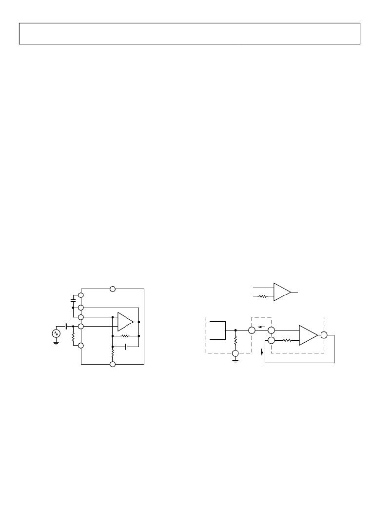
�high� dc� accuracy.� Figure� 34� shows� a� block� diagram� of� the� basic�
�amplifier� and� I/O� pins.� The� amplifier� is� often� configured� as� a� unity�
�gain� follower� but� is� easily� configured� for� gain,� as� a� Sallen-Key� low-�
�pass� filter� (in� conjunction� with� the� built-in� 16� k� I-to-V� resistor).�
�Note� that� an� additional� 16� k?� on-chip� precision� resistor� in� series�
�with� the� inverting� input� of� the� amplifier� balances� output� offset�
�voltages� resulting� from� the� bias� current� from� the� noninverting�
�amplifier.� The� output� buffer� is� disconnected� from� Pin� OUT� for�
�precision� core� measurements.�
�As� with� the� input� FET� buffer,� the� amplifier� positive� supply� is�
�disconnected� when� not� needed.� In� normal� circumstances,� the�
��shows� the� signal� connections� to� the� output� buffer.� Note� that�
�the� input� offset� voltage� contribution� by� the� bias� currents� are�
�balanced� by� equal� value� series� resistors,� resulting� in� near� zero�
�lowest� operating� frequency.� Figure� 33� is� a� schematic� showing�
�internal� components� and� pin� connections.�
�16�
�offset� voltage.�
�OBUFIN+�
�OUTPUT� BUFFER�
�+�
�2� RMS�
�IBUFV+�
�OBUFIN–�
�16k?�
�–�
�OBUFOUT�
�10μF�
�3�
�4�
�IBUFOUT�
�IBUFIN–�
�–�
�Figure� 34.� Output� Buffer� Block� Diagram�
�0.47μF�
�5�
�IBUFIN+�
�+�
�10k?�
�CORE�
�OUT�
�9�
�IBIAS�
�12�
�OBUFIN+�
�+�
�OBUFOUT�
�10M?�
�10pF�
�16k?�
�13�
�16k?�
�–�
�14�
�11� IGND�
�OBUFIN–�
�6�
�10k?�
�OGND�
�8�
�IBUFGN�
�Figure� 33.� Connecting� the� FET� Input� Buffer�
�Capacitor� coupling� at� the� input� and� output� of� the� FET� buffer� is�
�recommended� to� avoid� transferring� the� buffer� offset� voltage� to�
�the� output.� Although� the� FET� input� impedance� is� extremely� high,�
�the� 10� M� centering� resistor� connected� to� IGND� must� be� taken�
�into� account� when� selecting� an� input� capacitor� value.� This� is� simply�
�an� impedance� calculation� using� the� lowest� desired� frequency,�
�and� finding� a� capacitor� value� based� on� the� least� attenuation� desired.�
�Figure� 35.� Basic� Output� Buffer� Connections�
�For� applications� requiring� ripple� suppression� in� addition� to� the�
�single-pole� output� filter� described� previously,� the� output� buffer�
�is� configurable� as� a� two-pole� Sallen-Key� filter� using� two� external�
�resistors� and� two� capacitors.� At� just� over� 100� kHz,� the� amplifier�
�has� enough� bandwidth� to� function� as� an� active� filter� for� low�
�frequencies� such� as� power� line� ripple.� For� a� modest� savings� in�
�cost� and� complexity,� the� external� 16� k� feedback� resistor� can� be�
�omitted,� resulting� in� slightly� higher� V� OS� (80� μV).�
�Rev.� B� |� Page� 14� of� 24�
�相关PDF资料 |
PDF描述 |
|---|---|
| PMLL4148L,115 | DIODE SW GPP 75V 200MA SOD80C |
| LP2980AIM5-4.7 | IC REG LDO 4.7V 50MA SOT23-5 |
| EMM36DRMI-S288 | CONN EDGECARD 72POS .156 EXTEND |
| IDT70T631S12DD | IC SRAM 4MBIT 12NS 144TQFP |
| RCA10DCBN | CONN EDGECARD 20POS R/A .125 SLD |
相关代理商/技术参数 |
参数描述 |
|---|---|
| AD8436BCPZ-RL | 功能描述:IC CONV TRUE RMS-DC LP 20LFCSP RoHS:是 类别:集成电路 (IC) >> PMIC - RMS 至 DC 转换器 系列:- 标准包装:46 系列:- 电流 - 电源:1.2mA 电源电压:±18 V,36 V 安装类型:表面贴装 封装/外壳:16-SOIC(0.295",7.50mm 宽) 供应商设备封装:16-SOIC W 包装:管件 |
| AD8436BCPZ-WP | 功能描述:IC CONV TRUE RMS-DC LP 20LFCSP RoHS:是 类别:集成电路 (IC) >> PMIC - RMS 至 DC 转换器 系列:- 标准包装:46 系列:- 电流 - 电源:1.2mA 电源电压:±18 V,36 V 安装类型:表面贴装 封装/外壳:16-SOIC(0.295",7.50mm 宽) 供应商设备封装:16-SOIC W 包装:管件 |
| AD8436BRQZ | 功能描述:其他电源管理 Low PowerTrue RMS-to-DC Converter RoHS:否 制造商:Texas Instruments 输出电压范围: 输出电流:4 mA 输入电压范围:3 V to 3.6 V 输入电流: 功率耗散: 工作温度范围:- 40 C to + 110 C 安装风格:SMD/SMT 封装 / 箱体:VQFN-48 封装:Reel |
| AD8436BRQZ_PROMO | 制造商:Analog Devices 功能描述:IC RMS TO DC CONV 0.5% QSOP |
| AD8436BRQZ-R7 | 功能描述:其他电源管理 Low PowerTrue RMS-to-DC Converter RoHS:否 制造商:Texas Instruments 输出电压范围: 输出电流:4 mA 输入电压范围:3 V to 3.6 V 输入电流: 功率耗散: 工作温度范围:- 40 C to + 110 C 安装风格:SMD/SMT 封装 / 箱体:VQFN-48 封装:Reel |
发布紧急采购,3分钟左右您将得到回复。