参数资料
| 型号: | AD845SQ |
| 厂商: | Analog Devices Inc |
| 文件页数: | 11/12页 |
| 文件大小: | 0K |
| 描述: | IC OPAMP JFET 16MHZ PREC 8CDIP |
| 标准包装: | 1 |
| 放大器类型: | J-FET |
| 电路数: | 1 |
| 转换速率: | 100 V/µs |
| 增益带宽积: | 16MHz |
| 电流 - 输入偏压: | 750pA |
| 电压 - 输入偏移: | 250µV |
| 电流 - 电源: | 10mA |
| 电流 - 输出 / 通道: | 50mA |
| 电压 - 电源,单路/双路(±): | ±4.75 V ~ 18 V |
| 工作温度: | -55°C ~ 125°C |
| 安装类型: | 通孔 |
| 封装/外壳: | 8-CDIP(0.300",7.62mm) |
| 供应商设备封装: | 8-CERDIP |
| 包装: | 管件 |
AD845
REV. E
–8–
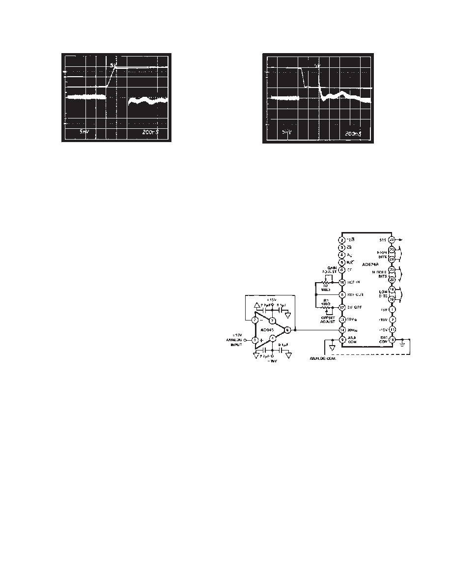
Figure 5. Settling Time of the 3-Op Amp Instrumentation
Amplifier. Horizontal Scale is 200 ns/Div, Vertical Scale,
Positive Pulse Input is 5 V/Div and Output Settling is
1 mV/Div.
Figure 6. Settling Time of the Three Op Amp Instru-
mentation Amplifier. Horizontal Scale: 200 ns/Div; Vertical
Scale, Negative Pulse Input: 5 V/ Div; Output Settling:
1 mV/Div.
DRIVING THE ANALOG INPUT OF AN A/D CONVERTER
An op amp driving the analog input of an A/D converter, such
as that shown in Figure 7, must be capable of maintaining a
constant output voltage under dynamically changing load condi-
tions. In successive approximation converters, the input current
is compared to a series of switched trial currents. The compari-
son point is diode clamped but may deviate several hundred
millivolts, resulting in high frequency modulation of A/D input
current. The output impedance of a feedback amplifier is made
artificially low by the loop gain. At high frequencies, where the
loop gain is low, the amplifier output impedance can approach
its open-loop value. Most IC amplifiers exhibit a minimum
open-loop output impedance of 25
W due to current limiting
resistors. A few hundred microamps reflected from the change
in converter loading can introduce errors in instantaneous input
voltage. If the A/D conversion speed is not excessive and the
bandwidth of the amplifier is sufficient, the amplifier’s output
will return to the nominal value before the converter makes its
comparison. However, many amplifiers have relatively narrow
bandwidth, yielding slow recovery from output transients. The
AD845 is ideally suited to drive high resolution A/D converters
with 5
ms or longer conversion times since it offers both wide
bandwidth and high open-loop gain.
Figure 7. AD845 As ADC Unity Gain Buffer
相关PDF资料 |
PDF描述 |
|---|---|
| AD8475ACPZ-R7 | IC FUNNEL AMP DIFF PREC 16LFCSP |
| AD8476ARMZ-R7 | IC AMP DIFF ADC DVR 8MSOP |
| AD847SQ | IC OPAMP GP 50MHZ LP 32MA 8CDIP |
| AD848SQ | IC OPAMP GP 175MHZ LP 32MA 8CDIP |
| AD8500AKSZ-R2 | IC OPAMP GP R-R CMOS 7KHZ SC70-5 |
相关代理商/技术参数 |
参数描述 |
|---|---|
| AD845SQ/883B | 制造商:Analog Devices 功能描述:OP Amp Single GP 制造商:Analog Devices 功能描述:OP AMP SGL GP 18V 8CDIP - Rail/Tube 制造商:Analog Devices Inc. 功能描述:Precision Amplifiers PRECISION 16MHZ H.S. AMP |
| AD846 | 制造商:AD 制造商全称:Analog Devices 功能描述:450 V/us, Precision, Current-Feedback Op Amp |
| AD8465 | 制造商:AD 制造商全称:Analog Devices 功能描述:Rail-to-Rail, Very Fast, 2.5 V to 5.5 V, Single-Supply LVDS Comparator |
| AD8465WBCPZ-R7 | 功能描述:IC COMPARATOR LVDS R-R 12LFCSP RoHS:是 类别:集成电路 (IC) >> 线性 - 比较器 系列:- 产品培训模块:Lead (SnPb) Finish for COTS Obsolescence Mitigation Program 标准包装:2,500 系列:- 类型:通用 元件数:1 输出类型:CMOS,推挽式,满摆幅,TTL 电压 - 电源,单路/双路(±):2.5 V ~ 5.5 V,±1.25 V ~ 2.75 V 电压 - 输入偏移(最小值):5mV @ 5.5V 电流 - 输入偏压(最小值):1pA @ 5.5V 电流 - 输出(标准):- 电流 - 静态(最大值):24µA CMRR, PSRR(标准):80dB CMRR,80dB PSRR 传输延迟(最大):450ns 磁滞:±3mV 工作温度:-40°C ~ 85°C 封装/外壳:6-WFBGA,CSPBGA 安装类型:表面贴装 包装:管件 其它名称:Q3554586 |
| AD8465WBCPZ-WP | 功能描述:IC COMPARATOR 1CH LVDS 12LFCSP RoHS:是 类别:集成电路 (IC) >> 线性 - 比较器 系列:- 产品培训模块:Lead (SnPb) Finish for COTS Obsolescence Mitigation Program 标准包装:50 系列:- 类型:带电压基准 元件数:4 输出类型:开路漏极 电压 - 电源,单路/双路(±):2.5 V ~ 11 V,±1.25 V ~ 5.5 V 电压 - 输入偏移(最小值):10mV @ 5V 电流 - 输入偏压(最小值):- 电流 - 输出(标准):0.015mA @ 5V 电流 - 静态(最大值):8.5µA CMRR, PSRR(标准):80dB CMRR,80dB PSRR 传输延迟(最大):- 磁滞:- 工作温度:0°C ~ 70°C 封装/外壳:16-SOIC(0.154",3.90mm 宽) 安装类型:表面贴装 包装:管件 产品目录页面:1386 (CN2011-ZH PDF) |
发布紧急采购,3分钟左右您将得到回复。