- 您现在的位置:买卖IC网 > PDF目录16928 > AD8475-EVALZ (Analog Devices Inc)BOARD EVAL FOR AD8475 PDF资料下载
参数资料
| 型号: | AD8475-EVALZ |
| 厂商: | Analog Devices Inc |
| 文件页数: | 10/24页 |
| 文件大小: | 0K |
| 描述: | BOARD EVAL FOR AD8475 |
| 标准包装: | 1 |
| 每 IC 通道数: | 1 - 单 |
| 放大器类型: | 差分 |
| 输出类型: | 差分,满摆幅 |
| 转换速率: | 50 V/µs |
| -3db带宽: | 150MHz |
| 电流 - 输出 / 通道: | 110mA |
| 工作温度: | -40°C ~ 85°C |
| 电流供应(主 IC): | 3mA |
| 电压 - 电源,单路/双路(±): | 3 V ~ 10 V,±1.5 V ~ 5 V |
| 板类型: | 完全填充 |
| 已供物品: | 板 |
| 已用 IC / 零件: | AD8475 |
AD8475
Data Sheet
Rev. C | Page 18 of 24
INPUT VOLTAGE RANGE
The AD8475 can measure input voltages that are larger than the
supply rails. The internal gain and feedback resistors form a
divider, which reduces the input voltage seen by the internal
input nodes of the amplifier. The largest voltage that can be
measured is constrained by the capability of the amplifier’s
internal summing nodes. This voltage is defined by the input
voltage and the ratio between the feedback and the gain resistors.
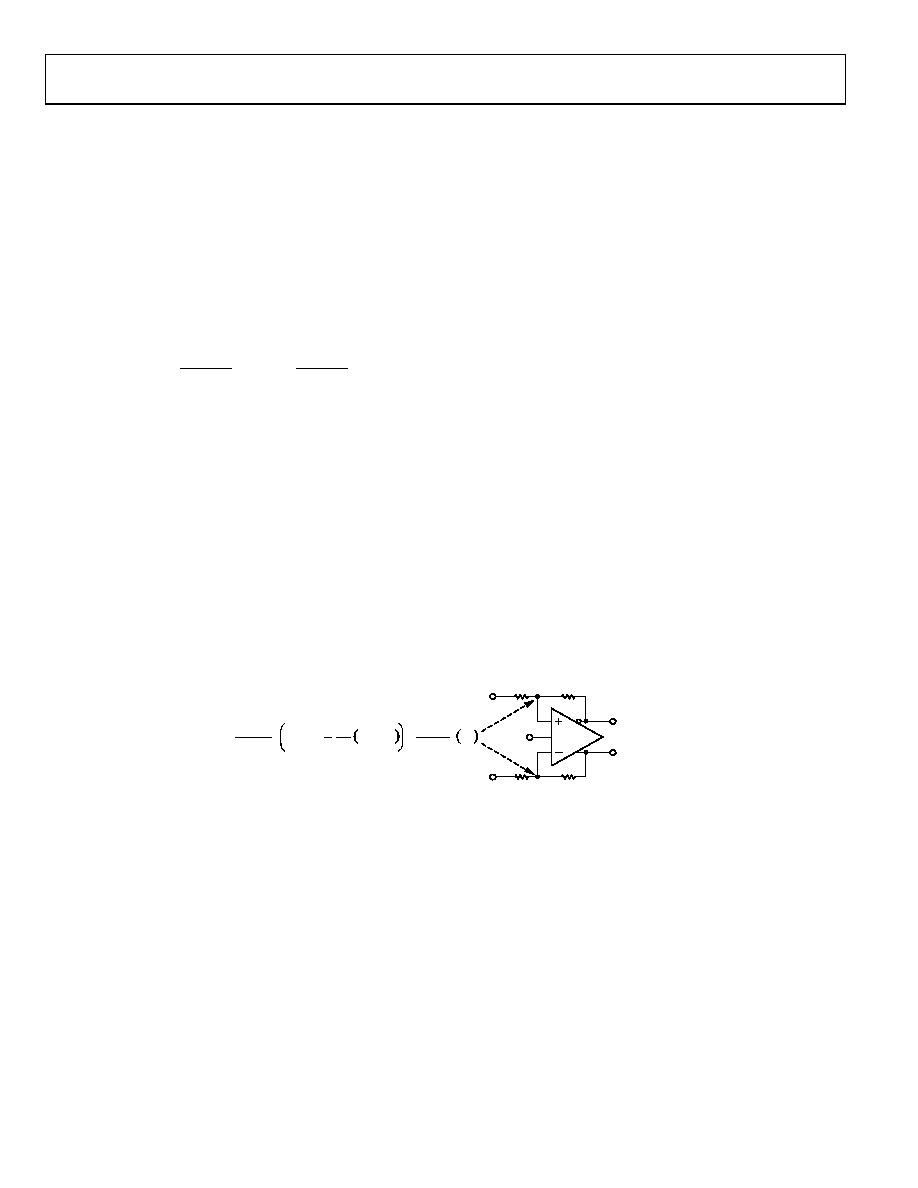
Figure 51 shows the voltage at the internal summing nodes of
the amplifier, defined by the input voltage and internal resistor
network. Written in terms of the input and output common-
mode voltages, this equation simplifies to
cm
IN
cm
OUT
MINUS
PLUS
V
RG
RF
V
RG
RF
RG
V
,
For the AD8475, RF is 1 kΩ, and RG is either 2.5 kΩ for G = 0.4
or 1.25 kΩ when G = 0.8 is used.
The internal amplifier of the AD8475 has rail-to-rail inputs. To
obtain accurate measurements with minimal distortion, the
voltage at the internal inputs of the amplifier must stay below
+VS 1 V and above VS.
For example, with VS = 5 V in a G = 0.4 configuration, the
AD8475 can measure a single-ended input as high as ±12.5 V
and maintain its excellent distortion performance.
The AD8475 provides overvoltage protection for excessive input
voltages beyond the supply rails. Integrated ESD protection diodes
and VS 16 V.
DRIVING THE AD8475
Care should be taken to drive the AD8475 with a low
impedance source: for example, another amplifier. Source
resistance can unbalance the resistor ratios and, therefore,
significantly degrade the gain accuracy and common-mode
rejection of the AD8475. For the best performance, source
impedance to the AD8475 input terminals should be kept
below 0.1 Ω. Refer to the DC Precision section for details on
the critical role of resistor ratios in the precision of the AD8475.
POWER SUPPLIES
The AD8475 operates over a wide range of supply voltages. It
can be powered on a single supply as low as 3 V and as high as
10 V. The AD8475 can also operate on dual supplies from
±1.5 V up to ±5 V
A stable dc voltage should be used to power the AD8475. Note
that noise on the supply pins can adversely affect performance.
For more information, see the PSRR performance curve in
Place a bypass capacitor of 0.1 μF between each supply pin and
ground, as close as possible to each supply pin. Use a tantalum
capacitor of 10 μF between each supply and ground. It can be
farther away from the supply pins and, typically, it can be
shared by other precision integrated circuits.
RF
RG
VON
VOP
VOCM
VP
VN
VN
RF + RG
RF
VP VN
RG
RF
VVOCM
RF + RG
RG
+
2
1
09
432
-16
4
Figure 51. Voltages at the Internal Op Amp Inputs of the AD8475
相关PDF资料 |
PDF描述 |
|---|---|
| PM105SB-471K-RC | INDUCTOR POWER 470UH SHIELD SMD |
| MIC2004-0.8YML TR | IC DISTRIBUTION SW 0.8A 2X2-MLF |
| 820131-000 | BOOT MOLDED |
| 2-556731-4 | CABLE ASSY PWR-LINE 8 WIRE 300" |
| ADA4841-2YR-EBZ | BOARD EVAL FOR ADA4841-2YR |
相关代理商/技术参数 |
参数描述 |
|---|---|
| AD8476 | 制造商:AD 制造商全称:Analog Devices 功能描述:Low Power, Unity Gain, Fully |
| AD8476ACPZ-R7 | 功能描述:IC AMP DIFF ADC DVR 16LFCSP RoHS:是 类别:集成电路 (IC) >> Linear - Amplifiers - Instrumentation 系列:- 标准包装:1 系列:- 放大器类型:通用 电路数:4 输出类型:满摆幅 转换速率:0.6 V/µs 增益带宽积:1MHz -3db带宽:- 电流 - 输入偏压:2pA 电压 - 输入偏移:1000µV 电流 - 电源:85µA 电流 - 输出 / 通道:20mA 电压 - 电源,单路/双路(±):1.8 V ~ 6 V 工作温度:-40°C ~ 125°C 安装类型:表面贴装 封装/外壳:14-SOIC(0.154",3.90mm 宽) 供应商设备封装:14-SOICN 包装:剪切带 (CT) 产品目录页面:680 (CN2011-ZH PDF) 其它名称:MCP6L04T-E/SLCT |
| AD8476ACPZ-R7_PROMO | 制造商:Analog Devices 功能描述:IC OP-AMP DIFF 6MHZ 10V/US |
| AD8476ACPZ-RL | 功能描述:IC AMP DIFF ADC DVR 16LFCSP RoHS:是 类别:集成电路 (IC) >> Linear - Amplifiers - Instrumentation 系列:- 标准包装:50 系列:LinCMOS™ 放大器类型:通用 电路数:4 输出类型:- 转换速率:0.05 V/µs 增益带宽积:110kHz -3db带宽:- 电流 - 输入偏压:0.7pA 电压 - 输入偏移:210µV 电流 - 电源:57µA 电流 - 输出 / 通道:30mA 电压 - 电源,单路/双路(±):3 V ~ 16 V,±1.5 V ~ 8 V 工作温度:-40°C ~ 85°C 安装类型:表面贴装 封装/外壳:14-SOIC(0.154",3.90mm 宽) 供应商设备封装:14-SOIC 包装:管件 产品目录页面:865 (CN2011-ZH PDF) 其它名称:296-1834296-1834-5 |
| AD8476ACPZ-WP | 功能描述:差分放大器 Low Power Unity Gain & ADC Driver RoHS:否 制造商:Analog Devices 通道数量:1 Channel 带宽:900 MHz 可用增益调整:5.6 dB to 20 dB 输入补偿电压:1 mV at 5 V 共模抑制比(最小值):67 dB 工作电源电压:11 V 电源电流:28 mA 最大工作温度:+ 85 C 最小工作温度:- 40 C 安装风格:SMD/SMT 封装 / 箱体:SOIC-8 封装:Reel |
发布紧急采购,3分钟左右您将得到回复。