- 您现在的位置:买卖IC网 > PDF目录5408 > AD8510ARM-R2 (Analog Devices Inc)IC OPAMP JFET 8MHZ PREC LN 8MSOP PDF资料下载
参数资料
| 型号: | AD8510ARM-R2 |
| 厂商: | Analog Devices Inc |
| 文件页数: | 9/20页 |
| 文件大小: | 0K |
| 描述: | IC OPAMP JFET 8MHZ PREC LN 8MSOP |
| 设计资源: | Versatile High Precision Programmable Current Sources Using DACs, Op Amps, and MOSFET Transistors (CN0151) |
| 标准包装: | 1 |
| 放大器类型: | J-FET |
| 电路数: | 1 |
| 转换速率: | 20 V/µs |
| 增益带宽积: | 8MHz |
| 电流 - 输入偏压: | 25pA |
| 电压 - 输入偏移: | 100µV |
| 电流 - 电源: | 2.2mA |
| 电流 - 输出 / 通道: | 70mA |
| 电压 - 电源,单路/双路(±): | ±4.5 V ~ 18 V |
| 工作温度: | -40°C ~ 125°C |
| 安装类型: | 表面贴装 |
| 封装/外壳: | 8-TSSOP,8-MSOP(0.118",3.00mm 宽) |
| 供应商设备封装: | 8-MSOP |
| 包装: | 标准包装 |
| 其它名称: | AD8510ARM-R2DKR |
AD8510/AD8512/AD8513
Rev. I | Page 17 of 20
I-V CONVERSION APPLICATIONS
Photodiode Circuits
Common applications for I-V conversion include photodiode
circuits where the amplifier is used to convert a current emitted
by a diode placed at the positive input terminal into an output
voltage.
The AD8510/AD8512/AD8513’s low input bias current, wide
bandwidth, and low noise make them each an excellent choice
for various photodiode applications, including fax machines,
fiber optic controls, motion sensors, and bar code readers.
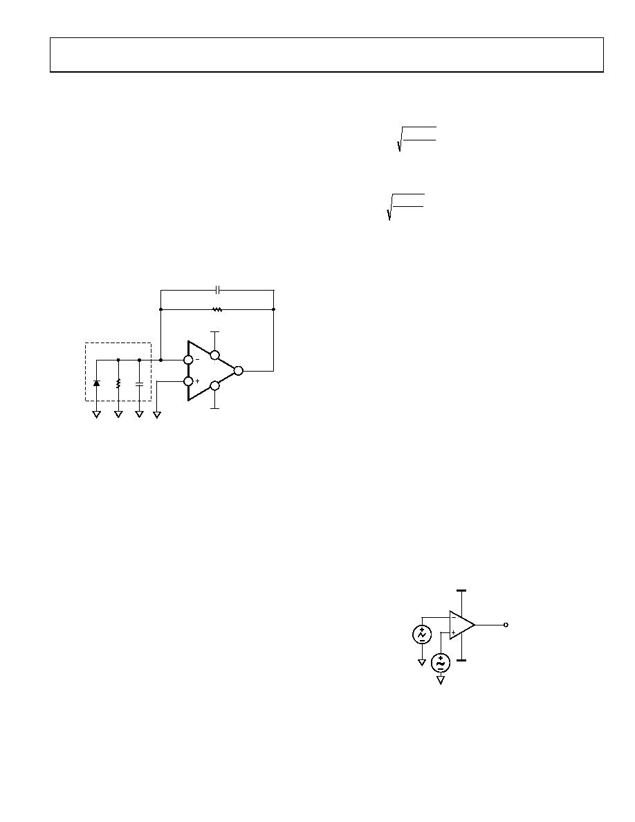
The circuit shown in Figure 53 uses a silicon diode with zero
bias voltage. This is known as a photovoltaic mode; this
configuration limits the overall noise and is suitable for
instrumentation applications.
4
7
3
6
2
AD8510
Cf
R2
Rd
Ct
VEE
VCC
02
72
9-
0
48
Figure 53. Equivalent Preamplifier Photodiode Circuit
A larger signal bandwidth can be attained at the expense of
additional output noise. The total input capacitance (Ct)
consists of the sum of the diode capacitance (typically 3 pF to
4 pF) and the amplifier’s input capacitance (12 pF), which
includes external parasitic capacitance. Ct creates a pole in the
frequency response that can lead to an unstable system. To
ensure stability and optimize the bandwidth of the signal, a
capacitor is placed in the feedback loop of the circuit shown in
Figure 53. It creates a zero and yields a bandwidth whose corner
frequency is 1/(2π(R2Cf)).
The value of R2 can be determined by the ratio
V
/ID
where:
V
is the desired output voltage of the op amp.
ID
is the diode current.
For example, if ID is 100 μA and a 10 V output voltage is desired,
R2 should be 100 kΩ. Rd (see Figure 53) is a junction resistance
that drops typically by a factor of 2 for every 10°C increase in
temperature.
A typical value for Rd is 1000 MΩ. Because Rd >> R2, the
circuit behavior is not impacted by the effect of the junction
resistance. The maximum signal bandwidth is
Ct
R
ft
f
MAX
2
2π
=
where ft is the unity gain frequency of the amplifier.
Cf can be calculated by
ft
R
Ct
Cf
2
2π
=
where ft is the unity gain frequency of the op amp, and it achieves
a phase margin, φM, of approximately 45°.
A higher phase margin can be obtained by increasing the value
of Cf. Setting Cf to twice the previous value yields approximately
φM = 65° and a maximal flat frequency response, but it reduces the
maximum signal bandwidth by 50%.
Using the previous parameters with a Cf ≈ 1 pF, the signal
bandwidth is approximately 2.6 MHz.
Signal Transmission Applications
One popular signal transmission method uses pulse-width
modulation. High data rates may require a fast comparator
rather than an op amp. However, the need for sharp, undistorted
signals may favor using a linear amplifier.
The AD8510/AD8512/AD8513 make excellent voltage
comparators. In addition to a high slew rate, the AD8510/
AD8512/AD8513 have a very fast saturation recovery time. In
the absence of feedback, the amplifiers are in open-loop mode
(very high gain). In this mode of operation, they spend much of
their time in saturation.
The circuit shown in Figure 54 was used to compare two signals
of different frequencies, namely a 100 Hz sine wave and a 1 kHz
triangular wave. Figure 55 shows a scope plot of the resulting
output waveforms. A pull-up resistor (typically 5 kΩ) can be
connected from the output to VCC if the output voltage needs to
reach the positive rail. The trade-off is that power consumption
is higher.
VOUT
V1
V2
4
2
6
7
3
–15V
+15V
02
72
9-
0
49
Figure 54. Pulse-Width Modulator
相关PDF资料 |
PDF描述 |
|---|---|
| SMF75AT1G | TVS ZENER 175W 75V SOD123FL |
| LTC2054IS5#TRMPBF | IC OPAMP 0-DRIFT SGL LP TSOT23-5 |
| MMB25-0051R1 | CONN RACK/PANEL 5POS 5A |
| SMF70AT1G | TVS ZENER 175W 70V SOD123FL |
| LTC2054IS5#TRM | IC OPAMP 0-DRIFT SGL LP TSOT23-5 |
相关代理商/技术参数 |
参数描述 |
|---|---|
| AD8510ARM-REEL | 制造商:Analog Devices 功能描述:OP Amp Single GP 制造商:Analog Devices 功能描述:OP Amp Single GP ±15V 8-Pin MSOP T/R |
| AD8510ARMZ | 功能描述:IC OPAMP JFET 8MHZ PREC LN 8MSOP RoHS:是 类别:集成电路 (IC) >> Linear - Amplifiers - Instrumentation 系列:- 标准包装:1,000 系列:- 放大器类型:电压反馈 电路数:4 输出类型:满摆幅 转换速率:33 V/µs 增益带宽积:20MHz -3db带宽:30MHz 电流 - 输入偏压:2nA 电压 - 输入偏移:3000µV 电流 - 电源:2.5mA 电流 - 输出 / 通道:30mA 电压 - 电源,单路/双路(±):4.5 V ~ 16.5 V,±2.25 V ~ 8.25 V 工作温度:-40°C ~ 85°C 安装类型:表面贴装 封装/外壳:14-SOIC(0.154",3.90mm 宽) 供应商设备封装:14-SOIC 包装:带卷 (TR) |
| AD8510ARMZ-R2 | 功能描述:IC OPAMP JFET 8MHZ PREC LN 8MSOP RoHS:是 类别:集成电路 (IC) >> Linear - Amplifiers - Instrumentation 系列:- 标准包装:2,500 系列:- 放大器类型:通用 电路数:1 输出类型:满摆幅 转换速率:0.11 V/µs 增益带宽积:350kHz -3db带宽:- 电流 - 输入偏压:4nA 电压 - 输入偏移:20µV 电流 - 电源:260µA 电流 - 输出 / 通道:20mA 电压 - 电源,单路/双路(±):2.7 V ~ 36 V,±1.35 V ~ 18 V 工作温度:-40°C ~ 85°C 安装类型:表面贴装 封装/外壳:8-SOIC(0.154",3.90mm 宽) 供应商设备封装:8-SO 包装:带卷 (TR) |
| AD8510ARMZ-REEL | 功能描述:IC OPAMP JFET 8MHZ PREC LN 8MSOP RoHS:是 类别:集成电路 (IC) >> Linear - Amplifiers - Instrumentation 系列:- 产品培训模块:Differential Circuit Design Techniques for Communication Applications 标准包装:1 系列:- 放大器类型:RF/IF 差分 电路数:1 输出类型:差分 转换速率:9800 V/µs 增益带宽积:- -3db带宽:2.9GHz 电流 - 输入偏压:3µA 电压 - 输入偏移:- 电流 - 电源:40mA 电流 - 输出 / 通道:- 电压 - 电源,单路/双路(±):3 V ~ 3.6 V 工作温度:-40°C ~ 85°C 安装类型:表面贴装 封装/外壳:16-VQFN 裸露焊盘,CSP 供应商设备封装:16-LFCSP-VQ 包装:剪切带 (CT) 产品目录页面:551 (CN2011-ZH PDF) 其它名称:ADL5561ACPZ-R7CT |
| AD8510AR-REEL | 制造商:Analog Devices 功能描述:OP Amp Single GP 制造商:Analog Devices 功能描述:OP Amp Single GP ±15V 8-Pin SOIC N T/R |
发布紧急采购,3分钟左右您将得到回复。