- 您现在的位置:买卖IC网 > PDF目录5241 > AD8510BRZ-REEL (Analog Devices Inc)IC OPAMP JFET 8MHZ PREC LN 8SOIC PDF资料下载
参数资料
| 型号: | AD8510BRZ-REEL |
| 厂商: | Analog Devices Inc |
| 文件页数: | 7/20页 |
| 文件大小: | 0K |
| 描述: | IC OPAMP JFET 8MHZ PREC LN 8SOIC |
| 设计资源: | Versatile High Precision Programmable Current Sources Using DACs, Op Amps, and MOSFET Transistors (CN0151) |
| 标准包装: | 2,500 |
| 放大器类型: | J-FET |
| 电路数: | 1 |
| 转换速率: | 20 V/µs |
| 增益带宽积: | 8MHz |
| 电流 - 输入偏压: | 25pA |
| 电压 - 输入偏移: | 80µV |
| 电流 - 电源: | 2.2mA |
| 电流 - 输出 / 通道: | 70mA |
| 电压 - 电源,单路/双路(±): | ±4.5 V ~ 18 V |
| 工作温度: | -40°C ~ 125°C |
| 安装类型: | 表面贴装 |
| 封装/外壳: | 8-SOIC(0.154",3.90mm 宽) |
| 供应商设备封装: | 8-SO |
| 包装: | 带卷 (TR) |
AD8510/AD8512/AD8513
Rev. I | Page 15 of 20
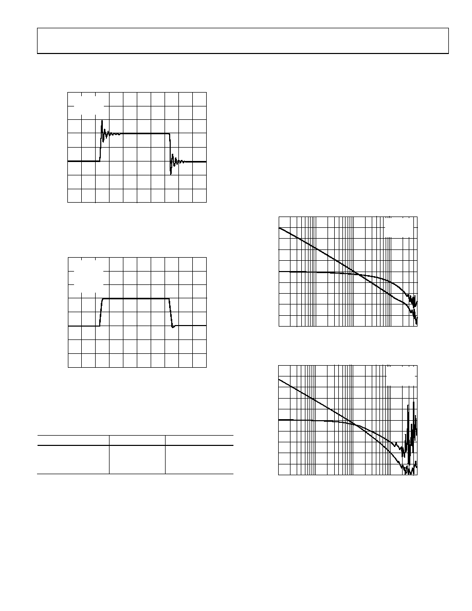
Figure 46 shows a scope plot of the output of the AD8510/AD8512/
AD8513 in response to a 400 mV pulse. The circuit is configured in
positive unity gain (worst case) with a load experience of 500 pF.
TIME (1s/DIV)
V
O
LT
A
GE
(
20
0m
V
/D
IV
)
VSY = ±15V
CL = 500pF
RL =10k
02
72
9-
0
41
Figure 46. Capacitive Load Drive Without Snubber
When the snubber circuit is used, the overshoot is reduced from
55% to less than 3% with the same load capacitance. Ringing is
virtually eliminated, as shown in Figure 47.
TIME (1s/DIV)
VO
LT
AG
E
(
200m
V
/DI
V
)
VSY = ±15V
RL = 10k
CL = 500pF
RS = 100
CS = 1nF
02
72
9-
04
2
Figure 47. Capacitive Load with Snubber Network
Optimum values for RS and CS depend on the load capacitance
and input stray capacitance and are determined empirically.
Table 5 shows a few values that can be used as starting points.
Table 5. Optimum Values for Capacitive Loads
CLOAD
RS (Ω)
CS
500 pF
100
1 nF
2 nF
70
100 pF
5 nF
60
300 pF
OPEN-LOOP GAIN AND PHASE RESPONSE
In addition to their impressive low noise, low offset voltage, and
offset current, the AD8510/AD8512/AD8513 have excellent
loop gain and phase response even when driving large resistive
and capacitive loads.
Compared with Competitor A (see Figure 49) under the same
conditions, with a 2.5 kΩ load at the output, the AD8510/AD8512/
AD8513 have more than 8 MHz of bandwidth and a phase margin
of more than 52°.
Competitor A, on the other hand, has only 4.5 MHz of band-
width and 28° of phase margin under the same test conditions.
Even with a 1 nF capacitive load in parallel with the 2 kΩ load
at the output, the AD8510/AD8512/AD8513 show much better
response than Competitor A, whose phase margin is degraded
to less than 0, indicating oscillation.
FREQUENCY (Hz)
G
A
IN
(
d
B
)
10k
–30
–20
–10
100k
0
10
30
1M
10M
50M
40
50
20
60
70
–135
–90
–45
0
45
90
135
180
225
270
315
P
HAS
E
(
D
eg
rees
)
02
72
9-
04
3
VSY = ±15V
RL = 2.5k
CL = 0pF
Figure 48. Frequency Response of the AD8510/AD8512/AD8513
FREQUENCY (Hz)
GA
IN
(
d
B
)
10k
–30
–20
–10
100k
0
10
30
1M
10M
50M
40
50
20
60
70
–135
–90
–45
0
45
90
135
180
225
270
315
P
H
AS
E
(
D
eg
rees)
02
72
9-
0
44
VSY = ±15V
RL = 2.5k
CL = 0pF
Figure 49. Frequency Response of Competitor A
相关PDF资料 |
PDF描述 |
|---|---|
| AD8052AR-REEL7 | IC OPAMP VF R-R DUAL LDIST 8SOIC |
| AD8056AR-REEL7 | IC OPAMP VF DUAL LDIST LN 8SOIC |
| OP249GS-REEL7 | IC OPAMP JFET 4.7MHZ DUAL 8SOIC |
| OP295GSZ-REEL7 | IC OPAMP GP R-R 85KHZ DUAL 8SOIC |
| LT6202HS5#TRPBF | IC OP AMP RRIO 100MHZ TSOT23-5 |
相关代理商/技术参数 |
参数描述 |
|---|---|
| AD8510BRZ-REEL7 | 功能描述:IC OPAMP JFET 8MHZ PREC LN 8SOIC RoHS:是 类别:集成电路 (IC) >> Linear - Amplifiers - Instrumentation 系列:- 其它有关文件:Automotive Product Guide 产品培训模块:Lead (SnPb) Finish for COTS Obsolescence Mitigation Program 标准包装:1 系列:- 放大器类型:通用 电路数:1 输出类型:满摆幅 转换速率:3 V/µs 增益带宽积:10MHz -3db带宽:- 电流 - 输入偏压:1pA 电压 - 输入偏移:70µV 电流 - 电源:2.5mA 电流 - 输出 / 通道:48mA 电压 - 电源,单路/双路(±):2.7 V ~ 5.5 V,±1.35 V ~ 2.75 V 工作温度:-40°C ~ 125°C 安装类型:表面贴装 封装/外壳:SOT-23-6 供应商设备封装:SOT-6 包装:Digi-Reel® 其它名称:MAX4475AUT#TG16DKR |
| AD8511 | 制造商:AD 制造商全称:Analog Devices 功能描述:9- and 11-Channel, Muxed Input LCD Reference Drivers |
| AD8511ACPZ-REEL | 制造商:Rochester Electronics LLC 功能描述: 制造商:Analog Devices 功能描述: |
| AD8511ARU | 制造商:AD 制造商全称:Analog Devices 功能描述:9- and 11-Channel, Muxed Input LCD Reference Drivers |
| AD8511ARU-REEL | 制造商:Analog Devices 功能描述:LCD DRVR 5V 48-Pin TSSOP T/R 制造商:Rochester Electronics LLC 功能描述:11-CHANNEL LCD REFERENCE DRIVER - Tape and Reel |
发布紧急采购,3分钟左右您将得到回复。