- 您现在的位置:买卖IC网 > PDF目录373947 > AD8512ARZ-REEL7 (ANALOG DEVICES INC) AC 7C 7#16S PIN RECP PDF资料下载
参数资料
| 型号: | AD8512ARZ-REEL7 |
| 厂商: | ANALOG DEVICES INC |
| 元件分类: | 运动控制电子 |
| 英文描述: | AC 7C 7#16S PIN RECP |
| 中文描述: | DUAL OP-AMP, 1800 uV OFFSET-MAX, 8 MHz BAND WIDTH, PDSO8 |
| 封装: | ROHS COMPLIANT, MS-012AA, SOIC-8 |
| 文件页数: | 14/20页 |
| 文件大小: | 497K |
| 代理商: | AD8512ARZ-REEL7 |
AD8510/AD8512/AD8513
SETTLING TIME
Settling time is the time it takes the output of the amplifier to
reach and remain within a percentage of its final value after a
pulse has been applied at the input. The AD8510/AD8512/
AD8513 settle to within 0.01% in less than 900 ns with a step of
0 V to 10 V in unity gain. This makes the each of the parts an
excellent choice as a buffer at the output of DACs whose settling
time is typically less than 1 μs.
Rev. E | Page 14 of 20
In addition to their fast settling time and fast slew rate, the
AD8510/AD8512/AD8513’s low offset voltage drift and input
offset current maintain full accuracy of 12-bit converters over
the entire operating temperature range.
OVERLOAD RECOVERY TIME
Overload recovery, also known as overdrive recovery, is the time
it takes the output of an amplifier to recover from a saturated
condition to its linear region. This recovery time is particularly
important in applications where the amplifier must amplify
small signals in the presence of large transient voltages.
Figure 43 shows the positive overload recovery of the
AD8510/AD8512/AD8513. The output recovers in
approximately 200 ns from a saturated condition.
TIME (2
μ
s/DIV)
V
200mV
0V
0V
–15V
0
I
O
V
SY
= ±15V
V
IN
= 200mV
A
= –100
RL = 10k
Figure 43. Positive Overload Recovery
The negative overdrive recovery time shown in Figure 44 is less
than 200 ns.
In addition to the fast recovery time, the AD8510/AD8512/
AD8513 show excellent symmetry of the positive and negative
recovery times. This is an important feature for transient signal
rectification, because the output signal is kept equally undis-
torted throughout any given period.
TIME (2
μ
s/DIV)
V
–200mV
0V
0V
+15V
0
I
O
V
SY
= ±15V
A
V
= –100
R
L
= 10k
Figure 44. Negative Overload Recovery
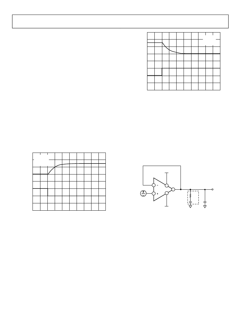
CAPACITIVE LOAD DRIVE
The AD8510/AD8512/AD8513 are unconditionally stable at all
gains in inverting and noninverting configurations. They are
capable of driving up to 1000 pF of capacitive loads without
oscillation in unity gain, the worst-case configuration.
However, as with most amplifiers, driving larger capacitive loads
in a unity gain configuration may cause excessive overshoot and
ringing or even oscillation. A simple snubber network reduces
the amount of overshoot and ringing significantly. The advan-
tage of this configuration is that the output swing of the ampli-
fier is not reduced, because R
S
is outside the feedback loop.
7
4
6
AD8510
200mV
R
S
C
S
C
L
V
OUT
V+
V–
0
Figure 45. Snubber Network Configuration
Figure 46 shows a scope photograph of the output of the
AD8510/AD8512/AD8513 in response to a 400 mV pulse. The
circuit is configured in positive unity gain (worst-case) with a
load experience of 500 pF.
相关PDF资料 |
PDF描述 |
|---|---|
| AD8512BR | Precision, Very Low Noise, Low Input Bias Current, Wide Bandwidth JFET Operational Amplifiers |
| AD8512BR-REEL | Precision, Very Low Noise, Low Input Bias Current, Wide Bandwidth JFET Operational Amplifiers |
| AD8512BR-REEL7 | Precision, Very Low Noise, Low Input Bias Current, Wide Bandwidth JFET Operational Amplifiers |
| AD8510ARZ-REEL7 | Precision, Very Low Noise, Low Input Bias Current, Wide Bandwidth JFET Operational Amplifiers |
| AD8510BR-REEL | JOYSTICK 4000 POTENTIOMETER |
相关代理商/技术参数 |
参数描述 |
|---|---|
| AD8512BR | 功能描述:IC OPAMP JFET 8MHZ DUAL LN 8SOIC RoHS:否 类别:集成电路 (IC) >> Linear - Amplifiers - Instrumentation 系列:- 标准包装:2,500 系列:Excalibur™ 放大器类型:J-FET 电路数:1 输出类型:- 转换速率:45 V/µs 增益带宽积:10MHz -3db带宽:- 电流 - 输入偏压:20pA 电压 - 输入偏移:490µV 电流 - 电源:1.7mA 电流 - 输出 / 通道:48mA 电压 - 电源,单路/双路(±):4.5 V ~ 38 V,±2.25 V ~ 19 V 工作温度:-40°C ~ 85°C 安装类型:表面贴装 封装/外壳:8-SOIC(0.154",3.90mm 宽) 供应商设备封装:8-SOIC 包装:带卷 (TR) |
| AD8512BR-REEL | 功能描述:IC OPAMP JFET 8MHZ DUAL LN 8SOIC RoHS:否 类别:集成电路 (IC) >> Linear - Amplifiers - Instrumentation 系列:- 标准包装:150 系列:- 放大器类型:音频 电路数:2 输出类型:- 转换速率:5 V/µs 增益带宽积:12MHz -3db带宽:- 电流 - 输入偏压:100nA 电压 - 输入偏移:500µV 电流 - 电源:6mA 电流 - 输出 / 通道:50mA 电压 - 电源,单路/双路(±):4 V ~ 32 V,±2 V ~ 16 V 工作温度:-40°C ~ 85°C 安装类型:表面贴装 封装/外壳:8-TSSOP(0.173",4.40mm 宽) 供应商设备封装:8-TSSOP 包装:管件 |
| AD8512BR-REEL7 | 功能描述:IC OPAMP JFET 8MHZ DUAL LN 8SOIC RoHS:否 类别:集成电路 (IC) >> Linear - Amplifiers - Instrumentation 系列:- 标准包装:150 系列:- 放大器类型:音频 电路数:2 输出类型:- 转换速率:5 V/µs 增益带宽积:12MHz -3db带宽:- 电流 - 输入偏压:100nA 电压 - 输入偏移:500µV 电流 - 电源:6mA 电流 - 输出 / 通道:50mA 电压 - 电源,单路/双路(±):4 V ~ 32 V,±2 V ~ 16 V 工作温度:-40°C ~ 85°C 安装类型:表面贴装 封装/外壳:8-TSSOP(0.173",4.40mm 宽) 供应商设备封装:8-TSSOP 包装:管件 |
| AD8512BRZ | 功能描述:IC OPAMP JFET 8MHZ DUAL LN 8SOIC RoHS:是 类别:集成电路 (IC) >> Linear - Amplifiers - Instrumentation 系列:- 标准包装:2,500 系列:- 放大器类型:通用 电路数:4 输出类型:- 转换速率:0.6 V/µs 增益带宽积:1MHz -3db带宽:- 电流 - 输入偏压:45nA 电压 - 输入偏移:2000µV 电流 - 电源:1.4mA 电流 - 输出 / 通道:40mA 电压 - 电源,单路/双路(±):3 V ~ 32 V,±1.5 V ~ 16 V 工作温度:0°C ~ 70°C 安装类型:表面贴装 封装/外壳:14-TSSOP(0.173",4.40mm 宽) 供应商设备封装:14-TSSOP 包装:带卷 (TR) 其它名称:LM324ADTBR2G-NDLM324ADTBR2GOSTR |
| AD8512BRZ-REEL | 功能描述:IC OPAMP JFET 8MHZ DUAL LN 8SOIC RoHS:是 类别:集成电路 (IC) >> Linear - Amplifiers - Instrumentation 系列:- 标准包装:50 系列:- 放大器类型:J-FET 电路数:2 输出类型:- 转换速率:13 V/µs 增益带宽积:3MHz -3db带宽:- 电流 - 输入偏压:65pA 电压 - 输入偏移:3000µV 电流 - 电源:1.4mA 电流 - 输出 / 通道:- 电压 - 电源,单路/双路(±):7 V ~ 36 V,±3.5 V ~ 18 V 工作温度:-40°C ~ 85°C 安装类型:通孔 封装/外壳:8-DIP(0.300",7.62mm) 供应商设备封装:8-PDIP 包装:管件 |
发布紧急采购,3分钟左右您将得到回复。