- 您现在的位置:买卖IC网 > PDF目录6110 > AD8519ARTZ-REEL7 (Analog Devices Inc)IC OPAMP GP R-R 8MHZ SOT23-5 PDF资料下载
参数资料
| 型号: | AD8519ARTZ-REEL7 |
| 厂商: | Analog Devices Inc |
| 文件页数: | 4/16页 |
| 文件大小: | 0K |
| 描述: | IC OPAMP GP R-R 8MHZ SOT23-5 |
| 标准包装: | 1 |
| 放大器类型: | 通用 |
| 电路数: | 1 |
| 输出类型: | 满摆幅 |
| 转换速率: | 2.9 V/µs |
| 增益带宽积: | 8MHz |
| 电流 - 输入偏压: | 300nA |
| 电压 - 输入偏移: | 600µV |
| 电流 - 电源: | 600µA |
| 电流 - 输出 / 通道: | 25mA |
| 电压 - 电源,单路/双路(±): | 2.7 V ~ 12 V,±1.35 V ~ 6 V |
| 工作温度: | -40°C ~ 125°C |
| 安装类型: | 表面贴装 |
| 封装/外壳: | SC-74A,SOT-753 |
| 供应商设备封装: | SOT-23-5 |
| 包装: | 标准包装 |
| 产品目录页面: | 766 (CN2011-ZH PDF) |
| 其它名称: | AD8519ARTZ-REEL7DKR |
AD8519/AD8529
Rev. D | Page 12 of 16
APPLICATIONS INFORMATION
MAXIMUM POWER DISSIPATION
The maximum power that can be safely dissipated by the
AD8519/AD8529 is limited by the associated rise in junction
temperature. The maximum safe junction temperature is 150°C
for these plastic packages. If this maximum is momentarily
exceeded, proper circuit operation is restored as soon as the
die temperature is reduced. Operating the product in an
overheated condition for an extended period can result in
permanent damage to the device.
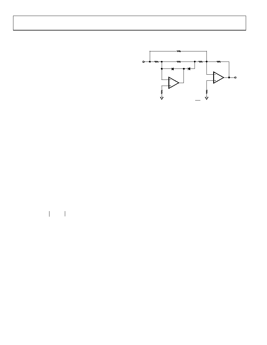
PRECISION FULL-WAVE RECTIFIER
Slew rate is probably the most underestimated parameter when
designing a precision rectifier. Yet without a good slew rate,
large glitches are generated during the period when both diodes
are off.
The operation of the basic circuit (shown in Figure 23) should
be examined before considering the slew rate further. U1 is set
up to have two states of operation. D1 and D2 diodes switch the
output between the two states. State one is an inverter with a
gain of +1, and state two is a simple unity gain buffer where the
output is equal to the value of the virtual ground. The virtual
ground is the potential present at the noninverting node of the
U1. State one is active when VIN is larger than the virtual
ground. D2 is on in this condition. If VIN drops below virtual
ground, D2 turns off and D1 turns on. This causes the output of
U1 to simply buffer the virtual ground and this configuration is
state two. Therefore, the function of U1, which results from
these two states of operation, is a half-wave inverter. The U2
function takes the inverted half wave at a gain of two and sums
it into the original VIN wave, which outputs a rectified full wave.
0
2
1
<
=
IN
OUT
V
This type of rectifier can be very precise if the following
electrical parameters are adhered to:
All passive components should be of tight tolerance, 1% for
resistors and 5% for capacitors.
If the application circuit requires high impedance (that is,
direct sensor interface), then an FET amplifier is a better
choice than the AD8519.
An amp such as the AD8519, which has a great slew rate
specification, yields the best result because the circuit
involves switching.
AD8519
U2
U1
VIRTUAL GROUND =
2
NODE A
VOUT
VCC
VIN
R1
10k
R4
10k
R2
10k
R3
4.99k
R5
10k
D2
1N914
D1
1N914
R7
3.32k
R6
5k
0175
6-
023
Figure 23. Precision Full-Wave Rectifier
Switching glitches are caused when D1 and D2 are both
momentarily off. This condition occurs every time the input
signal is equal to the virtual ground potential. When this
condition occurs, the U1 stage is taken out of the VOUT equation
and VOUT is equal to VIN × R5 × (R4 || R1 + R2 + R3). Note that
Node A should be VIN inverted or virtual ground, but in this
condition, Node A is simply tracking VIN. Given a sine wave
input centered around virtual ground, glitches are generated
at the sharp negative peaks of the rectified sine wave. If the
glitches are hard to notice on an oscilloscope, raise the fre-
quency of the sine wave until they become apparent. The size
of the glitches is proportional to the input frequency, the diode
turn-on potential (0.2 V or 0.65 V), and the slew rate of the op amp.
R6 and R7 are both necessary to limit the amount of bias
current related voltage offset. Unfortunately, there is no perfect
value for R6 because the impedance at the inverting node is
altered as D1 and D2 switch. Therefore, there is also some
unresolved bias current related offset. To minimize this offset,
use lower value resistors or choose an FET amplifier if the
optimized offset is still intolerable.
The AD8519 offers a unique combination of speed vs. power
ratio at 2.7 V single supply, small size (SC70 and SOT-23), and low
noise that makes it an ideal choice for most high volume and
high precision rectifier circuits.
相关PDF资料 |
PDF描述 |
|---|---|
| 0070.1461.B1 | AVTS VARISTOR 14VAC 14MM THT |
| 0070.1161.B1 | AVTS VARISTOR 11VAC 14MM THT |
| 0072.5141.B1 | AVTT VARISTOR 510VAC 10MM THT |
| ADA4062-2ACPZ-R7 | IC OPAMP JFET 1.4MHZ DL 10LFCSP |
| 0072.4841.B1 | AVTT VARISTOR 480VAC 10MM THT |
相关代理商/技术参数 |
参数描述 |
|---|---|
| AD8519ARZ | 功能描述:IC OPAMP GP R-R 8MHZ 25MA 8SOIC RoHS:是 类别:集成电路 (IC) >> Linear - Amplifiers - Instrumentation 系列:- 标准包装:2,500 系列:- 放大器类型:通用 电路数:1 输出类型:满摆幅 转换速率:0.11 V/µs 增益带宽积:350kHz -3db带宽:- 电流 - 输入偏压:4nA 电压 - 输入偏移:20µV 电流 - 电源:260µA 电流 - 输出 / 通道:20mA 电压 - 电源,单路/双路(±):2.7 V ~ 36 V,±1.35 V ~ 18 V 工作温度:-40°C ~ 85°C 安装类型:表面贴装 封装/外壳:8-SOIC(0.154",3.90mm 宽) 供应商设备封装:8-SO 包装:带卷 (TR) |
| AD8519ARZ-REEL | 功能描述:IC OPAMP GP R-R 8MHZ 25MA 8SOIC RoHS:是 类别:集成电路 (IC) >> Linear - Amplifiers - Instrumentation 系列:- 标准包装:2,500 系列:- 放大器类型:通用 电路数:1 输出类型:满摆幅 转换速率:0.11 V/µs 增益带宽积:350kHz -3db带宽:- 电流 - 输入偏压:4nA 电压 - 输入偏移:20µV 电流 - 电源:260µA 电流 - 输出 / 通道:20mA 电压 - 电源,单路/双路(±):2.7 V ~ 36 V,±1.35 V ~ 18 V 工作温度:-40°C ~ 85°C 安装类型:表面贴装 封装/外壳:8-SOIC(0.154",3.90mm 宽) 供应商设备封装:8-SO 包装:带卷 (TR) |
| AD8519ARZ-REEL7 | 功能描述:IC OPAMP GP R-R 8MHZ 25MA 8SOIC RoHS:是 类别:集成电路 (IC) >> Linear - Amplifiers - Instrumentation 系列:- 标准包装:2,500 系列:- 放大器类型:通用 电路数:1 输出类型:满摆幅 转换速率:0.11 V/µs 增益带宽积:350kHz -3db带宽:- 电流 - 输入偏压:4nA 电压 - 输入偏移:20µV 电流 - 电源:260µA 电流 - 输出 / 通道:20mA 电压 - 电源,单路/双路(±):2.7 V ~ 36 V,±1.35 V ~ 18 V 工作温度:-40°C ~ 85°C 安装类型:表面贴装 封装/外壳:8-SOIC(0.154",3.90mm 宽) 供应商设备封装:8-SO 包装:带卷 (TR) |
| AD8522 | 制造商:AD 制造商全称:Analog Devices 功能描述:+5 Volt, Serial Input, Dual 12-Bit DAC |
| AD8522ACPZ-REEL | 功能描述:IC DAC DUAL 12BIT 5V 制造商:analog devices inc. 系列:- 零件状态:上次购买时间 标准包装:1 |
发布紧急采购,3分钟左右您将得到回复。