- 您现在的位置:买卖IC网 > PDF目录373947 > AD8532 (Analog Devices, Inc.) Low Cost, 250 mA Output Single-Supply Amplifiers(低成本,250mA输出,单电源双放大器) PDF资料下载
参数资料
| 型号: | AD8532 |
| 厂商: | Analog Devices, Inc. |
| 英文描述: | Low Cost, 250 mA Output Single-Supply Amplifiers(低成本,250mA输出,单电源双放大器) |
| 中文描述: | 低成本,250 mA输出单电源放大器(低成本,250mA的输出,单电源双放大器) |
| 文件页数: | 9/16页 |
| 文件大小: | 220K |
| 代理商: | AD8532 |
AD8531/AD8532/AD8534
REV. A
–9–
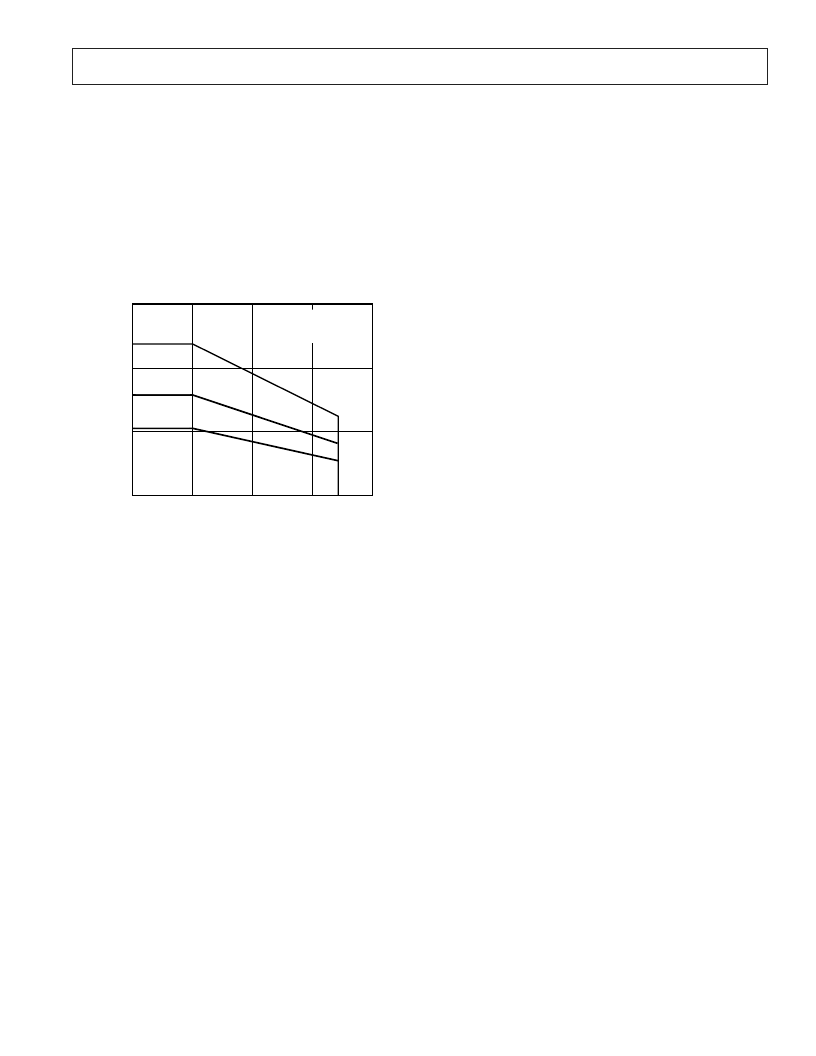
Power Dissipation
Although the AD8531/AD8532/AD8534 is capable of providing
load currents to 250 mA, the usable output load current drive
capability will be limited to the maximum power dissipation al-
lowed by the device package used. In any application, the abso-
lute maximum junction temperature for the AD8531/AD8532/
AD8534 is 150
°
C, and should never be exceeded for the device
could suffer premature failure. Accurately measuring power
dissipation of an integrated circuit is not always a straightfor-
ward exercise, so Figure 34 has been provided as a design aid
for either setting a safe output current drive level or in selecting
a heat sink for the three package options available on the
AD8531/AD8532/AD8534.
TEMPERATURE –
8
C
1.5
1
00
100
25
P
50
75
0.5
85
T
J
MAX = 150
8
C
FREE AIR
NO HEAT SINK
PDIP
θ
JA
= 103
8
C/W
SOIC
θ
JA
= 158
8
C/W
TSSOP
θ
JA
= 240
8
C/W
Figure 34. Maximum Power Dissipation vs. Ambient
Temperature
T hese thermal resistance curves were determined using the
AD8531/AD8532/AD8534 thermal resistance data for each
package and a maximum junction temperature of 150
°
C. T he fol-
lowing formula can be used to calculate the internal junction tem-
perature of the AD8531/AD8532/AD8534 for any application:
T
J
=
P
DISS
×
θ
J A
+ T
A
where
T
J
= junction temperature;
P
DISS
= power dissipation;
θ
J A
= package thermal resistance,
junction-to-case; and
T
A
= Ambient temperature of the circuit.
T o calculate the power dissipated by the AD8531/AD8532/
AD8534, the following equation can be used:
P
DISS
=
I
LOAD
×
(
V
S
–V
OUT
)
where
I
LOAD
= is output load current;
V
S
= is supply voltage; and
V
OUT
= is output voltage.
T he quantity within the parentheses is the maximum voltage
developed across either output transistor. As an additional de-
sign aid in calculating available load current from the AD8531/
AD8532/AD8534, Figure 1 illustrates the AD8531/AD8532/
AD8534 output voltage as a function of load resistance.
Power Calculations for Varying or Unknown Loads
Often, calculating power dissipated by an integrated circuit to
determine if the device is being operated in a safe range is not
as simple as it might seem. In many cases power cannot be
directly measured. T his may be the result of irregular output
waveforms or varying loads; indirect methods of measuring
power are required.
T here are two methods to calculate power dissipated by an in-
tegrated circuit. T he first can be done by measuring the pack-
age temperature and the board temperature. T he other is to
directly measure the circuit’s supply current.
C alculating Power by Measuring Ambient and C ase
T emperature
Given the two equations for calculating junction temperature:
T
J
=
T
A
+
P
θ
J A
where
T
J
is junction temperature, and
T
A
is ambient tempera-
ture.
θ
J A
is the junction to ambient thermal resistance.
T
J
=
T
C
+ P
θ
J C
where
T
C
is case temperature and
θ
J A
and
θ
J C
are given in the
data sheet.
T he two equations can be solved for
P
(power):
T
A
+
P
θ
J A
= T
C
+ P
θ
J C
P = (T
A
– T
C
)/ (
θ
J C
–
θ
J A
)
Once power has been determined it is necessary to go back and
calculate the junction temperature to assure that it has not
been exceeded.
T he temperature measurements should be directly on the
package and on a spot on the board that is near the package
but definitely not touching it. Measuring the package could be
difficult. A very small bimetallic junction glued to the package
could be used or it could be done using an infrared sensing
device if the spot size is small enough.
Calculating Power by Measuring Supply Current
Power can be calculated directly knowing the supply voltage
and current. However, supply current may have a dc compo-
nent with a pulse into a capacitive load. T his could make rms
current very difficult to calculate. It can be overcome by lifting
the supply pin and inserting an rms current meter into the cir-
cuit. For this to work you must be sure all of the current is be-
ing delivered by the supply pin you are measuring. T his is
usually a good method in a single supply system; however, if
the system uses dual supplies, both supplies may need to be
monitored.
Input Overvoltage Protection
As with any semiconductor device, whenever the condition ex-
ists for the input to exceed either supply voltage, the device’s
input overvoltage characteristic must be considered. When an
overvoltage occurs, the amplifier could be damaged depending
on the magnitude of the applied voltage and the magnitude of
the fault current. Although not shown here, when the input
voltage exceeds either supply by more than 0.6 V, pn-junctions
internal to the AD8531/AD8532/AD8534 energize allowing
current to flow from the input to the supplies. As illustrated in
the simplified equivalent input circuit (Figure 32), the AD8531/
AD8532/AD8534 does not have any internal current limiting
resistors, so fault currents can quickly rise to damaging levels.
T his input current is not inherently damaging to the device as
long as it is limited to 5 mA or less. For the AD8531/AD8532/
AD8534, once the input voltage exceeds the supply by more
than 0.6 V the input current quickly exceeds 5 mA. If this
相关PDF资料 |
PDF描述 |
|---|---|
| AD8534 | Low Cost, 250 mA Output Single-Supply Amplifiers(低成本,250mA输出,单电源四放大器) |
| AD8538_07 | Low Power, Precision, Auto-Zero Op Amps |
| AD8539 | Low Power, Precision, Auto-Zero Op Amps |
| AD8541AKS-R2 | General Purpose CMOS Rail-to-Rail Amplifiers |
| AD8541AKS-REEL7 | General Purpose CMOS Rail-to-Rail Amplifiers |
相关代理商/技术参数 |
参数描述 |
|---|---|
| AD8532AN | 制造商:Analog Devices 功能描述:OP AMP DUAL HIGH O/P RRI/O 8532 |
| AD8532AR | 功能描述:IC OPAMP GP R-R CMOS 3MHZ 8SOIC RoHS:否 类别:集成电路 (IC) >> Linear - Amplifiers - Instrumentation 系列:- 标准包装:160 系列:- 放大器类型:通用 电路数:4 输出类型:满摆幅 转换速率:10 V/µs 增益带宽积:9MHz -3db带宽:- 电流 - 输入偏压:1pA 电压 - 输入偏移:250µV 电流 - 电源:730µA 电流 - 输出 / 通道:28mA 电压 - 电源,单路/双路(±):2.7 V ~ 5.5 V,±1.35 V ~ 2.75 V 工作温度:-40°C ~ 125°C 安装类型:表面贴装 封装/外壳:16-SOIC(0.154",3.90mm 宽) 供应商设备封装:16-SOIC N 包装:管件 |
| AD8532ARM | 制造商:Analog Devices 功能描述: |
| AD8532ARM-R2 | 制造商:Analog Devices 功能描述:OP Amp Dual GP R-R I/O 6V 8-Pin MSOP T/R |
| AD8532ARM-REEL | 制造商:Analog Devices 功能描述:OP Amp Dual GP R-R I/O 6V 8-Pin MSOP T/R 制造商:Rochester Electronics LLC 功能描述:CMOS RAIL/RAIL INPUT/OUTPUT OP AMP - Tape and Reel |
发布紧急采购,3分钟左右您将得到回复。