- 您现在的位置:买卖IC网 > PDF目录6127 > AD8532ARMZ-REEL (Analog Devices Inc)IC OPAMP GP R-R CMOS 3MHZ 8MSOP PDF资料下载
参数资料
| 型号: | AD8532ARMZ-REEL |
| 厂商: | Analog Devices Inc |
| 文件页数: | 3/20页 |
| 文件大小: | 0K |
| 描述: | IC OPAMP GP R-R CMOS 3MHZ 8MSOP |
| 标准包装: | 1 |
| 放大器类型: | 通用 |
| 电路数: | 2 |
| 输出类型: | 满摆幅 |
| 转换速率: | 5 V/µs |
| 增益带宽积: | 3MHz |
| 电流 - 输入偏压: | 5pA |
| 电压 - 输入偏移: | 25000µV |
| 电流 - 电源: | 750µA |
| 电流 - 输出 / 通道: | 250mA |
| 电压 - 电源,单路/双路(±): | 2.7 V ~ 6 V,±1.35 V ~ 3 V |
| 工作温度: | -40°C ~ 85°C |
| 安装类型: | 表面贴装 |
| 封装/外壳: | 8-TSSOP,8-MSOP(0.118",3.00mm 宽) |
| 供应商设备封装: | 8-MSOP |
| 包装: | 标准包装 |
| 产品目录页面: | 766 (CN2011-ZH PDF) |
| 其它名称: | AD8532ARMZ-REELDKR |
AD8531/AD8532/AD8534
Rev. F | Page 11 of 20
THEORY OF OPERATION
The AD8531/AD8532/AD8534 are all CMOS, high output
current drive, rail-to-rail input/output operational amplifiers.
Their high output current drive and stability with heavy capacitive
loads make the AD8531/AD8532/AD8534 excellent choices as
drive amplifiers for LCD panels.
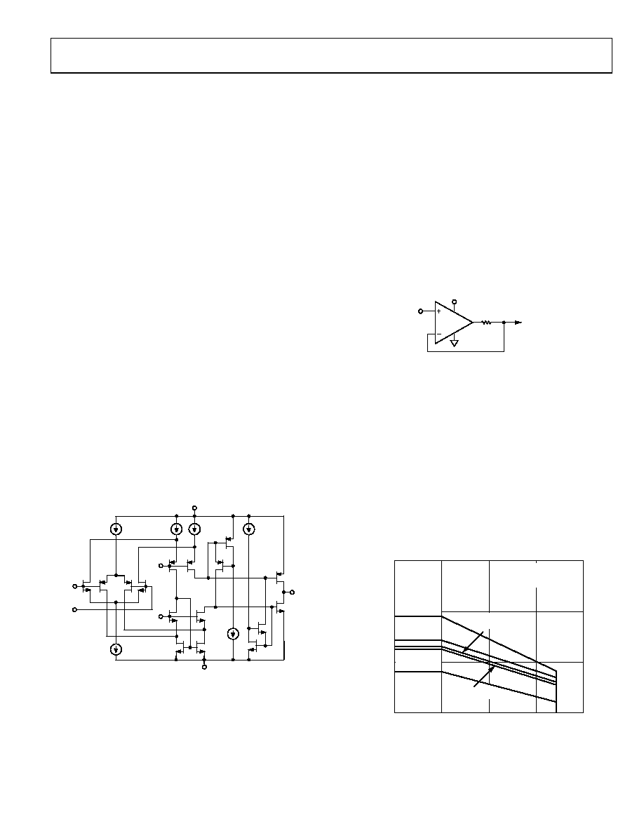
Figure 36 illustrates a simplified equivalent circuit for the
AD8531/AD8532/AD8534. Like many rail-to-rail input amplifier
configurations, it comprises two differential pairs, one N-channel
(M1 to M2) and one P-channel (M3 to M4). These differential
pairs are biased by 50 μA current sources, each with a compliance
limit of approximately 0.5 V from either supply voltage rail. The
differential input voltage is then converted into a pair of
differential output currents. These differential output currents
are then combined in a compound folded-cascade second gain
stage (M5 to M9). The outputs of the second gain stage at M8
and M9 provide the gate voltage drive to the rail-to-rail output
stage. Additional signal current recombination for the output
stage is achieved using M11 to M14.
To achieve rail-to-rail output swings, the AD8531/AD8532/
AD8534 design employs a complementary, common source
output stage (M15 to M16). However, the output voltage swing
is directly dependent on the load current because the difference
between the output voltage and the supply is determined by
the AD8531/AD8532/AD8534’s output transistors on channel
exhibits voltage gain by virtue of the use of common source
amplifiers; as a result, the voltage gain of the output stage (thus,
the open-loop gain of the device) exhibits a strong dependence
on the total load resistance at the output of the AD8531/
AD8532/AD8534.
50A
100A
20A
VB2
M5
M8
M12
M15
M16
M11
OUT
M3
M4 M2
M1
IN–
IN+
VB3
M6
M7
M10
20A
M13
50A
V+
V–
M9
M14
01
09
9-
0
36
Figure 36. Simplified Equivalent Circuit
SHORT-CIRCUIT PROTECTION
As a result of the design of the output stage for the maximum
load current capability, the AD8531/AD8532/AD8534 do not
have any internal short-circuit protection circuitry. Direct
connection of the output of the AD8531/AD8532/AD8534 to
the positive supply in single-supply applications destroys the
device. In applications where some protection is needed, but not
at the expense of reduced output voltage headroom, a low value
resistor in series with the output, as shown in Figure 37, can be
used. The resistor, connected within the feedback loop of the
amplifier, has very little effect on the performance of the amplifier
other than limiting the maximum available output voltage
swing. For single 5 V supply applications, resistors less than
20 Ω are not recommended.
5V
RX
20
VOUT
VIN
AD8532
01
09
9-
03
7
Figure 37. Output Short-Circuit Protection
POWER DISSIPATION
Although the AD8531/AD8532/AD8534 are capable of
providing load currents to 250 mA, the usable output load
current drive capability is limited to the maximum power
dissipation allowed by the device package used. In any
application, the absolute maximum junction temperature
for the AD8531/AD8532/AD8534 is 150°C. The maximum
junction temperature should never be exceeded because the
device could suffer premature failure. Accurately measuring
power dissipation of an integrated circuit is not always a
straightforward exercise; therefore, Figure 38 is provided
as a design aid for either setting a safe output current drive
level or selecting a heat sink for the package options available
on the AD8531/AD8532/AD8534.
TEMPERATURE (°C)
P
O
W
E
R
DI
S
IP
AT
IO
N
(
W
)
1.5
1.0
0.5
0
25
50
75
85
100
01
099
-03
8
TJ MAX = 150°C
FREE AIR
NO HEAT SINK
TSSOP
θJA = 240°C/W
SC70
θJA = 376°C/W
SOIC
θJA = 158°C/W
MSOP
θJA = 210°C/W
SOT-23
θJA = 230°C/W
Figure 38. Maximum Power Dissipation vs. Ambient Temperature
相关PDF资料 |
PDF描述 |
|---|---|
| 1-86479-0 | CONN HEADER RT/A 26POS .100 30AU |
| 963242-2000-AR-PT | CONN SOCKET DUAL 42POS GOLD SMD |
| VC080514A300RP | TVS CERAMIC 14V 0805 SMD |
| VC080512A250RP | TVS CERAMIC 12V 0805 SMD |
| BU7261G-TR | OP AMP I/O LV 1.8-5.5V 5-SSOP |
相关代理商/技术参数 |
参数描述 |
|---|---|
| AD8532AR-REEL | 功能描述:IC OPAMP GP R-R CMOS 3MHZ 8SOIC RoHS:否 类别:集成电路 (IC) >> Linear - Amplifiers - Instrumentation 系列:- 标准包装:160 系列:- 放大器类型:通用 电路数:4 输出类型:满摆幅 转换速率:10 V/µs 增益带宽积:9MHz -3db带宽:- 电流 - 输入偏压:1pA 电压 - 输入偏移:250µV 电流 - 电源:730µA 电流 - 输出 / 通道:28mA 电压 - 电源,单路/双路(±):2.7 V ~ 5.5 V,±1.35 V ~ 2.75 V 工作温度:-40°C ~ 125°C 安装类型:表面贴装 封装/外壳:16-SOIC(0.154",3.90mm 宽) 供应商设备封装:16-SOIC N 包装:管件 |
| AD8532ARREEL7 | 制造商:AD 功能描述:* |
| AD8532AR-REEL7 | 功能描述:IC OPAMP GP R-R CMOS 3MHZ 8SOIC RoHS:否 类别:集成电路 (IC) >> Linear - Amplifiers - Instrumentation 系列:- 标准包装:160 系列:- 放大器类型:通用 电路数:4 输出类型:满摆幅 转换速率:10 V/µs 增益带宽积:9MHz -3db带宽:- 电流 - 输入偏压:1pA 电压 - 输入偏移:250µV 电流 - 电源:730µA 电流 - 输出 / 通道:28mA 电压 - 电源,单路/双路(±):2.7 V ~ 5.5 V,±1.35 V ~ 2.75 V 工作温度:-40°C ~ 125°C 安装类型:表面贴装 封装/外壳:16-SOIC(0.154",3.90mm 宽) 供应商设备封装:16-SOIC N 包装:管件 |
| AD8532ARU | 制造商:Analog Devices 功能描述:OP Amp Dual GP R-R I/O 6V 8-Pin TSSOP 制造商:Rochester Electronics LLC 功能描述:CMOS RAIL/RAIL INPUT/OUTPUT OP AMP - Bulk |
| AD8532ARU-REEL | 功能描述:IC OPAMP GP R-R CMOS 3MHZ 8TSSOP RoHS:否 类别:集成电路 (IC) >> Linear - Amplifiers - Instrumentation 系列:- 标准包装:160 系列:- 放大器类型:通用 电路数:4 输出类型:满摆幅 转换速率:10 V/µs 增益带宽积:9MHz -3db带宽:- 电流 - 输入偏压:1pA 电压 - 输入偏移:250µV 电流 - 电源:730µA 电流 - 输出 / 通道:28mA 电压 - 电源,单路/双路(±):2.7 V ~ 5.5 V,±1.35 V ~ 2.75 V 工作温度:-40°C ~ 125°C 安装类型:表面贴装 封装/外壳:16-SOIC(0.154",3.90mm 宽) 供应商设备封装:16-SOIC N 包装:管件 |
发布紧急采购,3分钟左右您将得到回复。