参数资料
| 型号: | AD8552AR |
| 厂商: | Analog Devices Inc |
| 文件页数: | 13/24页 |
| 文件大小: | 0K |
| 描述: | IC OPAMP CHOPPER R-R DUAL 8SOIC |
| 产品培训模块: | Op Amp Basics |
| 标准包装: | 98 |
| 放大器类型: | 断路器(零漂移) |
| 电路数: | 2 |
| 输出类型: | 满摆幅 |
| 转换速率: | 0.4 V/µs |
| 增益带宽积: | 1.5MHz |
| 电流 - 输入偏压: | 10pA |
| 电压 - 输入偏移: | 1000µV |
| 电流 - 电源: | 850µA |
| 电流 - 输出 / 通道: | 30mA |
| 电压 - 电源,单路/双路(±): | 2.7 V ~ 5.5 V |
| 工作温度: | -40°C ~ 125°C |
| 安装类型: | 表面贴装 |
| 封装/外壳: | 8-SOIC(0.154",3.90mm 宽) |
| 供应商设备封装: | 8-SO |
| 包装: | 管件 |
AD8551/AD8552/AD8554
Data Sheet
Rev. E | Page 20 of 24
APPLICATIONS INFORMATION
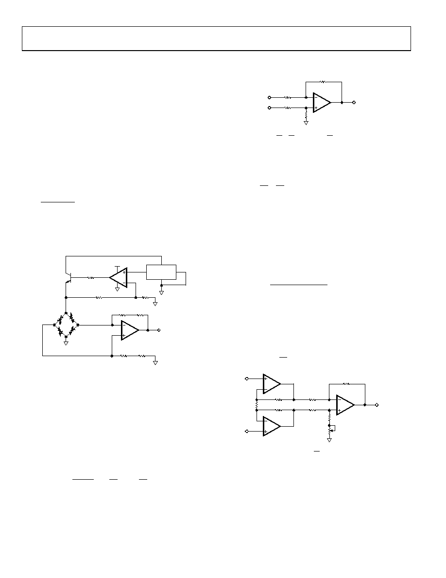
A 5 V PRECISION STRAIN GAGE CIRCUIT
The extremely low offset voltage of the AD8552 makes it an
ideal amplifier for any application requiring accuracy with high
gains, such as a weigh scale or strain gage. Figure 65 shows a
configuration for a single-supply, precision, strain gage
measurement system.
A REF192 provides a 2.5 V precision reference voltage for A2.
The A2 amplifier boosts this voltage to provide a 4.0 V reference
for the top of the strain gage resistor bridge. Q1 provides the
current drive for the 350 Ω bridge network. A1 is used to
amplify the output of the bridge with the full-scale output
voltage equal to
(
)
B
2
1
R
R +
×
2
(17)
where RB is the resistance of the load cell.
Using the values given in Figure 65, the output voltage linearly
varies from 0 V with no strain to 4.0 V under full strain.
NOTES
1. USE 0.1% TOLERANCE RESISTORS.
AD8552-A
AD8552-B
REF192
5V
2.5V
6
4
3
2
4.0V
A2
A1
VOUT
0V TO 4.0V
40mV
FULL-SCALE
Q1
2N2222
OR
EQUIVALENT
350
LOAD
CELL
1k
12.0k
20k
R1
17.4k
R2
100
R3
17.4k
R4
100
01101-
065
Figure 65. A 5 V Precision Strain Gage Amplifier
3 V INSTRUMENTATION AMPLIFIER
The high common-mode rejection, high open-loop gain, and
operation down to 3 V of supply voltage makes the AD855x
an excellent choice of op amp for discrete single-supply
instrumentation amplifiers. The common-mode rejection ratio
of the AD855x is greater than 120 dB, but the CMRR of the system
is also a function of the external resistor tolerances. The gain of
the difference amplifier shown in Figure 66 is given as
+
+
=
1
2
1
4
3
4
OUT
R
V
R
V
2
1
(18)
V2
V1
R1
R2
VOUT
AD8551/
AD8552/
AD8554
R3
R4
IF
R4
R3
R2
R1
R2
R1
=
, THEN VOUT =
× (V1 – V2)
01101-
066
Figure 66. Using the AD855x as a Difference Amplifier
In an ideal difference amplifier, the ratio of the resistors are set
exactly equal to
3
4
1
2
V
R
A
=
(19)
Which sets the output voltage of the system to
VOUT = AV(V1 V2)
(20)
Due to finite component tolerance, the ratio between the four
resistors is not exactly equal, and any mismatch results in a
reduction of common-mode rejection from the system. Referring
to Figure 66, the exact common-mode rejection ratio can be
expressed as
3
2
4
1
3
2
4
2
4
1
R
CMRR
2
+
=
(21)
In the three-op amp, instrumentation amplifier configuration
shown in Figure 67, the output difference amplifier is set to
unity gain with all four resistors equal in value. If the tolerance
of the resistors used in the circuit is given as δ, the worst-case
CMRR of the instrumentation amplifier is
δ
CMRRMIN
2
1
=
(22)
VOUT = 1 +
2R
RG
(V1 – V2)
R
AD8554-C
V2
R
V1
AD8554-B
AD8554-A
RTRIM
RG
VOUT
01101-
067
Figure 67. A Discrete Instrumentation Amplifier Configuration
Consequently, using 1% tolerance resistors results in a worst-case
system CMRR of 0.02, or 34 dB. Therefore, either high precision
resistors or an additional trimming resistor, as shown in Figure 67,
must be used to achieve high common-mode rejection. The
value of this trimming resistor must be equal to the value of R
multiplied by its tolerance. For example, using 10 kΩ resistors
with 1% tolerance requires a series trimming resistor equal to
100 Ω.
相关PDF资料 |
PDF描述 |
|---|---|
| TMM-137-01-G-D-SM | CONN HEADER 74POS DUAL 2MM SMD |
| 1.5KE110AHE3/54 | TVS UNIDIR 1.5KW 110V 5% 1.5KE |
| 1.5KE10AHE3/54 | TVS UNIDIR 1.5KW 10V 5% 1.5KE |
| 1.5KE100AHE3/54 | TVS UNIDIR 1.5KW 100V 5% 1.5KE |
| 929665-04-26-I | CONN HEADER .100 DUAL STR 52POS |
相关代理商/技术参数 |
参数描述 |
|---|---|
| AD8552AR-REEL | 功能描述:IC OPAMP CHOPPER R-R DUAL 8SOIC RoHS:否 类别:集成电路 (IC) >> Linear - Amplifiers - Instrumentation 系列:- 标准包装:50 系列:LinCMOS™ 放大器类型:通用 电路数:4 输出类型:- 转换速率:0.05 V/µs 增益带宽积:110kHz -3db带宽:- 电流 - 输入偏压:0.7pA 电压 - 输入偏移:210µV 电流 - 电源:57µA 电流 - 输出 / 通道:30mA 电压 - 电源,单路/双路(±):3 V ~ 16 V,±1.5 V ~ 8 V 工作温度:-40°C ~ 85°C 安装类型:表面贴装 封装/外壳:14-SOIC(0.154",3.90mm 宽) 供应商设备封装:14-SOIC 包装:管件 产品目录页面:865 (CN2011-ZH PDF) 其它名称:296-1834296-1834-5 |
| AD8552AR-REEL7 | 功能描述:IC OPAMP CHOPPER R-R DUAL 8SOIC RoHS:否 类别:集成电路 (IC) >> Linear - Amplifiers - Instrumentation 系列:- 其它有关文件:Automotive Product Guide 产品培训模块:Lead (SnPb) Finish for COTS Obsolescence Mitigation Program 标准包装:1 系列:- 放大器类型:通用 电路数:1 输出类型:满摆幅 转换速率:3 V/µs 增益带宽积:10MHz -3db带宽:- 电流 - 输入偏压:1pA 电压 - 输入偏移:70µV 电流 - 电源:2.5mA 电流 - 输出 / 通道:48mA 电压 - 电源,单路/双路(±):2.7 V ~ 5.5 V,±1.35 V ~ 2.75 V 工作温度:-40°C ~ 125°C 安装类型:表面贴装 封装/外壳:SOT-23-6 供应商设备封装:SOT-6 包装:Digi-Reel® 其它名称:MAX4475AUT#TG16DKR |
| AD8552ARU | 功能描述:IC OPAMP CHOPPER R-R DUAL 8TSSOP RoHS:否 类别:集成电路 (IC) >> Linear - Amplifiers - Instrumentation 系列:- 标准包装:73 系列:Over-The-Top® 放大器类型:通用 电路数:4 输出类型:满摆幅 转换速率:0.07 V/µs 增益带宽积:200kHz -3db带宽:- 电流 - 输入偏压:1nA 电压 - 输入偏移:285µV 电流 - 电源:50µA 电流 - 输出 / 通道:25mA 电压 - 电源,单路/双路(±):2 V ~ 44 V,±1 V ~ 22 V 工作温度:-40°C ~ 85°C 安装类型:表面贴装 封装/外壳:16-WFDFN 裸露焊盘 供应商设备封装:16-DFN-EP(5x3) 包装:管件 |
| AD8552ARU-REEL | 功能描述:IC OPAMP CHOPPER R-R DUAL 8TSSOP RoHS:否 类别:集成电路 (IC) >> Linear - Amplifiers - Instrumentation 系列:- 标准包装:50 系列:LinCMOS™ 放大器类型:通用 电路数:4 输出类型:- 转换速率:0.05 V/µs 增益带宽积:110kHz -3db带宽:- 电流 - 输入偏压:0.7pA 电压 - 输入偏移:210µV 电流 - 电源:57µA 电流 - 输出 / 通道:30mA 电压 - 电源,单路/双路(±):3 V ~ 16 V,±1.5 V ~ 8 V 工作温度:-40°C ~ 85°C 安装类型:表面贴装 封装/外壳:14-SOIC(0.154",3.90mm 宽) 供应商设备封装:14-SOIC 包装:管件 产品目录页面:865 (CN2011-ZH PDF) 其它名称:296-1834296-1834-5 |
| AD8552ARUZ | 功能描述:IC OPAMP CHOPPER R-R DUAL 8TSSOP RoHS:是 类别:集成电路 (IC) >> Linear - Amplifiers - Instrumentation 系列:- 标准包装:2,500 系列:- 放大器类型:通用 电路数:4 输出类型:- 转换速率:0.6 V/µs 增益带宽积:1MHz -3db带宽:- 电流 - 输入偏压:45nA 电压 - 输入偏移:2000µV 电流 - 电源:1.4mA 电流 - 输出 / 通道:40mA 电压 - 电源,单路/双路(±):3 V ~ 32 V,±1.5 V ~ 16 V 工作温度:0°C ~ 70°C 安装类型:表面贴装 封装/外壳:14-TSSOP(0.173",4.40mm 宽) 供应商设备封装:14-TSSOP 包装:带卷 (TR) 其它名称:LM324ADTBR2G-NDLM324ADTBR2GOSTR |
发布紧急采购,3分钟左右您将得到回复。