- 您现在的位置:买卖IC网 > PDF目录5264 > AD8552ARZ-REEL7 (Analog Devices Inc)IC OPAMP CHOPPER R-R DUAL 8SOIC PDF资料下载
参数资料
| 型号: | AD8552ARZ-REEL7 |
| 厂商: | Analog Devices Inc |
| 文件页数: | 9/24页 |
| 文件大小: | 0K |
| 描述: | IC OPAMP CHOPPER R-R DUAL 8SOIC |
| 产品培训模块: | Op Amp Basics |
| 标准包装: | 1,000 |
| 放大器类型: | 断路器(零漂移) |
| 电路数: | 2 |
| 输出类型: | 满摆幅 |
| 转换速率: | 0.4 V/µs |
| 增益带宽积: | 1.5MHz |
| 电流 - 输入偏压: | 10pA |
| 电压 - 输入偏移: | 1000µV |
| 电流 - 电源: | 850µA |
| 电流 - 输出 / 通道: | 30mA |
| 电压 - 电源,单路/双路(±): | 2.7 V ~ 5.5 V |
| 工作温度: | -40°C ~ 125°C |
| 安装类型: | 表面贴装 |
| 封装/外壳: | 8-SOIC(0.154",3.90mm 宽) |
| 供应商设备封装: | 8-SO |
| 包装: | 带卷 (TR) |
Data Sheet
AD8551/AD8552/AD8554
Rev. E | Page 17 of 24
1/f NOISE CHARACTERISTICS
Another advantage of auto-zero amplifiers is their ability to
cancel flicker noise. Flicker noise, also known as 1/f noise, is
noise inherent in the physics of semiconductor devices, and it
increases 3 dB for every octave decrease in frequency. The 1/f
corner frequency of an amplifier is the frequency at which the
flicker noise is equal to the broadband noise of the amplifier.
At lower frequencies, flicker noise dominates, causing higher
degrees of error for sub-Hertz frequencies or dc precision
applications.
Because the AD855x amplifiers are self-correcting op amps, they
do not have increasing flicker noise at lower frequencies. In
essence, low frequency noise is treated as a slowly varying offset
error and is greatly reduced as a result of autocorrection. The
correction becomes more effective as the noise frequency
approaches dc, offsetting the tendency of the noise to increase
exponentially as frequency decreases. This allows the AD855x
to have lower noise near dc than standard low noise amplifiers
that are susceptible to 1/f noise.
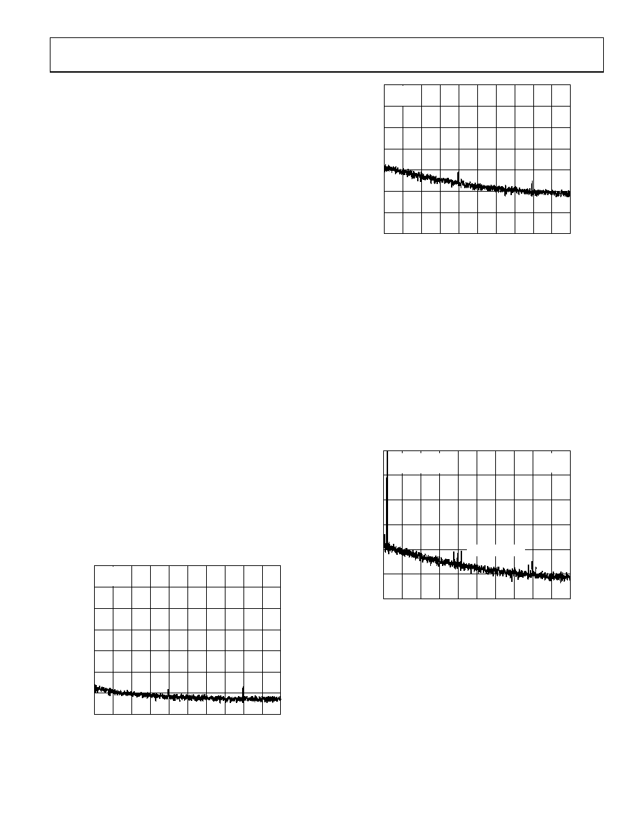
INTERMODULATION DISTORTION
The AD855x can be used as a conventional op amp for gain/
bandwidth combinations up to 1.5 MHz. The auto-zero correction
frequency of the device is fixed at 4 kHz. Although a trace amount
of this frequency feeds through to the output, the amplifier can
be used at much higher frequencies. Figure 56 shows the spectral
output of the AD8552 with the amplifier configured for unity
gain and the input grounded.
The 4 kHz auto-zero clock frequency appears at the output with
less than 2 μV of amplitude. Harmonics are also present, but at
reduced levels from the fundamental auto-zero clock frequency.
The amplitude of the clock frequency feedthrough is proportional
to the closed-loop gain of the amplifier. Like other autocorrection
amplifiers, at higher gains there is more clock frequency
feedthrough. Figure 57 shows the spectral output with the
amplifier configured for a gain of 60 dB.
FREQUENCY (kHz)
0
–140
0
10
1
OU
TP
U
T
S
IGN
A
L
(
dB
)
–20
–40
–60
–80
–100
–120
2
3
4
5
6
7
8
9
VSY = 5V
AV = 0dB
01101-
056
Figure 56. Spectral Analysis of AD8552 Output in Unity Gain Configuration
FREQUENCY (kHz)
0
–140
0
10
1
OU
TP
U
T
S
IGN
A
L
(
dB
)
–20
–40
–60
–80
–100
–120
2
3
4
5
6
7
8
9
VSY = 5V
AV = 60dB
01101-
057
Figure 57. Spectral Analysis of AD855x Output with +60 dB Gain
When an input signal is applied, the output contains some
degree of intermodulation distortion (IMD). This is another
characteristic feature of all autocorrection amplifiers. IMD
appears as sum and difference frequencies between the input
signal and the 4 kHz clock frequency (and its harmonics) and is
at a level similar to, or less than, the clock feedthrough at the
output. The IMD is also proportional to the closed-loop gain of
the amplifier. Figure 58 shows the spectral output of an AD8552
configured as a high gain stage (+60 dB) with a 1 mV input signal
applied. The relative levels of all IMD products and harmonic
distortion add up to produce an output error of 60 dB relative
to the input signal. At unity gain, these add up to only 120 dB
relative to the input signal.
IMD < 100V rms
OUTPUT SIGNAL
1V rms @ 200Hz
FREQUENCY (kHz)
0
10
1
OU
TP
U
T
S
IGN
A
L
(
dB
)
–20
–40
–60
–80
–100
–120
2
3
4
5
6
7
8
9
VSY = 5V
AV = 60dB
01101-
058
Figure 58. Spectral Analysis of AD8552 in High Gain with a 1 mV Input Signal
For most low frequency applications, the small amount of auto-
zero clock frequency feedthrough does not affect the precision
of the measurement system. If it is desired, the clock frequency
feedthrough can be reduced through the use of a feedback
capacitor around the amplifier. However, this reduces the
bandwidth of the amplifier. Figure 59 and Figure 60 show a
configuration for reducing the clock feedthrough and the
corresponding spectral analysis at the output. The 3 dB
bandwidth of this configuration is 480 Hz.
相关PDF资料 |
PDF描述 |
|---|---|
| 6-1879213-5 | RES 133 OHM 1/16W 0.1% 0402 |
| 0031.8516 | FUSE 2A 250VAC 5X20 FAST |
| 0031.8515 | FUSE 1.6A 250VAC 5X20 FAST |
| 2-1879208-7 | RES 120 OHM 1/16W 0.1% 0402 |
| 0702871123 | CONN HEADER BKWY DL GOLD 54POS |
相关代理商/技术参数 |
参数描述 |
|---|---|
| AD8553 | 制造商:AD 制造商全称:Analog Devices 功能描述:Wide Supply Range, Micropower, |
| AD85531 | 制造商:AD 制造商全称:Analog Devices 功能描述:10 MHz, 20 V/レs, G = 1, 10, 100, 1000 i CMOS㈢ Programmable Gain Instrumentation Amplifier |
| AD8553ARMZ | 功能描述:IC AMP INST R-R 1KHZ PREC 10MSOP RoHS:是 类别:集成电路 (IC) >> Linear - Amplifiers - Instrumentation 系列:- 产品培训模块:Differential Circuit Design Techniques for Communication Applications 标准包装:1 系列:- 放大器类型:RF/IF 差分 电路数:1 输出类型:差分 转换速率:9800 V/µs 增益带宽积:- -3db带宽:2.9GHz 电流 - 输入偏压:3µA 电压 - 输入偏移:- 电流 - 电源:40mA 电流 - 输出 / 通道:- 电压 - 电源,单路/双路(±):3 V ~ 3.6 V 工作温度:-40°C ~ 85°C 安装类型:表面贴装 封装/外壳:16-VQFN 裸露焊盘,CSP 供应商设备封装:16-LFCSP-VQ 包装:剪切带 (CT) 产品目录页面:551 (CN2011-ZH PDF) 其它名称:ADL5561ACPZ-R7CT |
| AD8553ARMZ-R2 | 功能描述:IC AMP INST R-R 1KHZ PREC 10MSOP RoHS:是 类别:集成电路 (IC) >> Linear - Amplifiers - Instrumentation 系列:- 标准包装:2,500 系列:- 放大器类型:通用 电路数:1 输出类型:满摆幅 转换速率:0.11 V/µs 增益带宽积:350kHz -3db带宽:- 电流 - 输入偏压:4nA 电压 - 输入偏移:20µV 电流 - 电源:260µA 电流 - 输出 / 通道:20mA 电压 - 电源,单路/双路(±):2.7 V ~ 36 V,±1.35 V ~ 18 V 工作温度:-40°C ~ 85°C 安装类型:表面贴装 封装/外壳:8-SOIC(0.154",3.90mm 宽) 供应商设备封装:8-SO 包装:带卷 (TR) |
| AD8553ARMZ-R2 | 制造商:Analog Devices 功能描述:Instrumentation Amplifier |
发布紧急采购,3分钟左右您将得到回复。