参数资料
| 型号: | AD8554ARUZ-REEL |
| 厂商: | Analog Devices Inc |
| 文件页数: | 10/24页 |
| 文件大小: | 0K |
| 描述: | IC OPAMP CHOPPER R-R 14TSSOP |
| 标准包装: | 2,500 |
| 放大器类型: | 断路器(零漂移) |
| 电路数: | 4 |
| 输出类型: | 满摆幅 |
| 转换速率: | 0.4 V/µs |
| 增益带宽积: | 1.5MHz |
| 电流 - 输入偏压: | 10pA |
| 电压 - 输入偏移: | 1000µV |
| 电流 - 电源: | 850µA |
| 电流 - 输出 / 通道: | 30mA |
| 电压 - 电源,单路/双路(±): | 2.7 V ~ 5.5 V |
| 工作温度: | -40°C ~ 125°C |
| 安装类型: | 表面贴装 |
| 封装/外壳: | 14-TSSOP(0.173",4.40mm 宽) |
| 供应商设备封装: | 14-TSSOP |
| 包装: | 带卷 (TR) |
AD8551/AD8552/AD8554
Data Sheet
Rev. E | Page 18 of 24
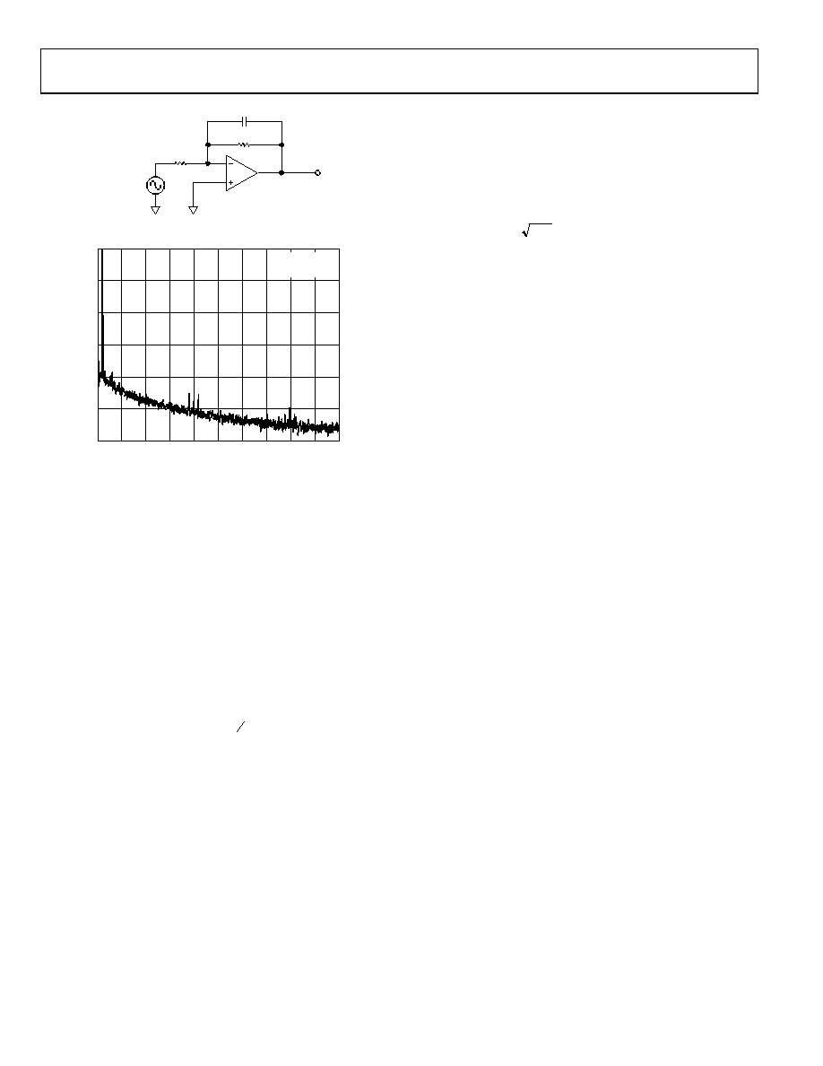
100
100k
3.3nF
VIN = 1mV rms
@ 200Hz
01101-
059
Figure 59. Reducing Autocorrection Clock Noise Using a Feedback Capacitor
FREQUENCY (kHz)
0
10
1
OU
TP
U
T
S
IGN
A
L
–20
–40
–60
–80
–100
–120
2
3
4
5
6
7
8
9
VSY = 5V
AV = 60dB
01101-
060
Figure 60. Spectral Analysis Using a Feedback Capacitor
BROADBAND AND EXTERNAL RESISTOR NOISE
CONSIDERATIONS
The total broadband noise output from any amplifier is primarily
a function of three types of noise: input voltage noise from the
amplifier, input current noise from the amplifier, and Johnson
noise from the external resistors used around the amplifier.
Input voltage noise, or en, is strictly a function of the amplifier
used. The Johnson noise from a resistor is a function of the re-
sistance and the temperature. Input current noise, or in, creates
an equivalent voltage noise proportional to the resistors used
around the amplifier. These noise sources are not correlated
with each other and their combined noise sums in a root-
squared-sum fashion. The full equation is given as
( )
[
] 21
2
_
4
S
n
S
n
TOTAL
n
R
i
kTr
e
+
=
(15)
Where:
en = the input voltage noise density of the amplifier.
in = the input current noise of the amplifier.
RS = source resistance connected to the noninverting terminal.
k = Boltzmann’s constant (1.38 × 10²³ J/K).
T = ambient temperature in Kelvin (K = 273.15 + °C).
The input voltage noise density (en) of the AD855x is 42 nV/√Hz,
and the input noise, in, is 2 fA/√Hz. The en,TOTAL is dominated by
the input voltage noise, provided the source resistance is less
than 106 kΩ. With source resistance greater than 106 kΩ, the
overall noise of the system is dominated by the Johnson noise of
the resistor itself.
Because the input current noise of the AD855x is very small,
it does not become a dominant term unless RS is greater than
4 GΩ, which is an impractical value of source resistance.
The total noise (en,TOTAL) is expressed in volts per square root
Hertz, and the equivalent rms noise over a certain bandwidth
can be found as
BW
e
TOTAL
n
×
=
,
(16)
where BW is the bandwidth of interest in Hertz.
OUTPUT OVERDRIVE RECOVERY
The AD855x amplifiers have an excellent overdrive recovery
of only 200 μs from either supply rail. This characteristic is
particularly difficult for autocorrection amplifiers because the
nulling amplifier requires a nontrivial amount of time to error
correct the main amplifier back to a valid output. Figure 29 and
Figure 30 show the positive and negative overdrive recovery
times for the AD855x.
The output overdrive recovery for an autocorrection amplifier is
defined as the time it takes for the output to correct to its final
voltage from an overload state. It is measured by placing the
amplifier in a high gain configuration with an input signal that
forces the output voltage to the supply rail. The input voltage is
then stepped down to the linear region of the amplifier, usually
to halfway between the supplies. The time from the input signal
stepdown to the output settling to within 100 μV of its final
value is the overdrive recovery time.
INPUT OVERVOLTAGE PROTECTION
Although the AD855x is a rail-to-rail input amplifier, exercise
care to ensure that the potential difference between the inputs
does not exceed 5 V. Under normal operating conditions, the
amplifier corrects its output to ensure the two inputs are at the
same voltage. However, if the device is configured as a comparator,
or is under some unusual operating condition, the input voltages
may be forced to different potentials. This can cause excessive
current to flow through internal diodes in the AD855x used to
protect the input stage against overvoltage.
If either input exceeds either supply rail by more than 0.3 V, large
amounts of current begin to flow through the ESD protection
diodes in the amplifier. These diodes connect between the inputs
and each supply rail to protect the input transistors against an
electrostatic discharge event and are normally reverse-biased.
However, if the input voltage exceeds the supply voltage, these
ESD diodes become forward-biased. Without current limiting,
excessive amounts of current can flow through these diodes,
causing permanent damage to the device. If inputs are subjected
to overvoltage, appropriate series resistors should be inserted to
limit the diode current to less than 2 mA maximum.
相关PDF资料 |
PDF描述 |
|---|---|
| PEC33DBEN | CONN HEADER .100 DUAL R/A 66POS |
| 125NHG01B | FUSE 125A 500V CLASS GL/GG |
| 160NHG01B | FUSE 160A 500V CLASS GL/GG |
| AD8554ARZ-REEL | IC OPAMP CHOPPER R-R QUAD 14SOIC |
| 929715-03-13-I | CONN HEADER .100 DUAL STR 26POS |
相关代理商/技术参数 |
参数描述 |
|---|---|
| AD8554ARZ | 功能描述:IC OPAMP CHOPPER R-R QUAD 14SOIC RoHS:是 类别:集成电路 (IC) >> Linear - Amplifiers - Instrumentation 系列:- 标准包装:2,500 系列:- 放大器类型:通用 电路数:4 输出类型:- 转换速率:0.6 V/µs 增益带宽积:1MHz -3db带宽:- 电流 - 输入偏压:45nA 电压 - 输入偏移:2000µV 电流 - 电源:1.4mA 电流 - 输出 / 通道:40mA 电压 - 电源,单路/双路(±):3 V ~ 32 V,±1.5 V ~ 16 V 工作温度:0°C ~ 70°C 安装类型:表面贴装 封装/外壳:14-TSSOP(0.173",4.40mm 宽) 供应商设备封装:14-TSSOP 包装:带卷 (TR) 其它名称:LM324ADTBR2G-NDLM324ADTBR2GOSTR |
| AD8554ARZ1 | 制造商:AD 制造商全称:Analog Devices 功能描述:Zero-Drift, Single-Supply, Rail-to-Rail Input/Output Operational Amplifiers |
| AD8554ARZ-REEL | 功能描述:IC OPAMP CHOPPER R-R QUAD 14SOIC RoHS:是 类别:集成电路 (IC) >> Linear - Amplifiers - Instrumentation 系列:- 标准包装:73 系列:Over-The-Top® 放大器类型:通用 电路数:4 输出类型:满摆幅 转换速率:0.07 V/µs 增益带宽积:200kHz -3db带宽:- 电流 - 输入偏压:1nA 电压 - 输入偏移:285µV 电流 - 电源:50µA 电流 - 输出 / 通道:25mA 电压 - 电源,单路/双路(±):2 V ~ 44 V,±1 V ~ 22 V 工作温度:-40°C ~ 85°C 安装类型:表面贴装 封装/外壳:16-WFDFN 裸露焊盘 供应商设备封装:16-DFN-EP(5x3) 包装:管件 |
| AD8554ARZ-REEL7 | 功能描述:IC OPAMP CHOPPER R-R QUAD 14SOIC RoHS:是 类别:集成电路 (IC) >> Linear - Amplifiers - Instrumentation 系列:- 标准包装:73 系列:Over-The-Top® 放大器类型:通用 电路数:4 输出类型:满摆幅 转换速率:0.07 V/µs 增益带宽积:200kHz -3db带宽:- 电流 - 输入偏压:1nA 电压 - 输入偏移:285µV 电流 - 电源:50µA 电流 - 输出 / 通道:25mA 电压 - 电源,单路/双路(±):2 V ~ 44 V,±1 V ~ 22 V 工作温度:-40°C ~ 85°C 安装类型:表面贴装 封装/外壳:16-WFDFN 裸露焊盘 供应商设备封装:16-DFN-EP(5x3) 包装:管件 |
| AD8555 | 制造商:AD 制造商全称:Analog Devices 功能描述:Zero-Drift, Digitally Programmable Sensor Signal Amplifier |
发布紧急采购,3分钟左右您将得到回复。