- 您现在的位置:买卖IC网 > PDF目录5895 > AD8556ARZ-REEL (Analog Devices Inc)IC AMP CHOPPER 2MHZ 10MA 8SOIC PDF资料下载
参数资料
| 型号: | AD8556ARZ-REEL |
| 厂商: | Analog Devices Inc |
| 文件页数: | 8/28页 |
| 文件大小: | 0K |
| 描述: | IC AMP CHOPPER 2MHZ 10MA 8SOIC |
| 标准包装: | 2,500 |
| 系列: | DigiTrim® |
| 放大器类型: | 断路器(零漂移) |
| 电路数: | 1 |
| 转换速率: | 1.2 V/µs |
| 增益带宽积: | 2MHz |
| 电流 - 输入偏压: | 49nA |
| 电压 - 输入偏移: | 2µV |
| 电流 - 电源: | 2mA |
| 电流 - 输出 / 通道: | 10mA |
| 电压 - 电源,单路/双路(±): | 4.5 V ~ 5.5 V |
| 工作温度: | -40°C ~ 140°C |
| 安装类型: | 表面贴装 |
| 封装/外壳: | 8-SOIC(0.154",3.90mm 宽) |
| 供应商设备封装: | 8-SO |
| 包装: | 带卷 (TR) |
第1页第2页第3页第4页第5页第6页第7页当前第8页第9页第10页第11页第12页第13页第14页第15页第16页第17页第18页第19页第20页第21页第22页第23页第24页第25页第26页第27页第28页
AD8556
Rev. A | Page 16 of 28
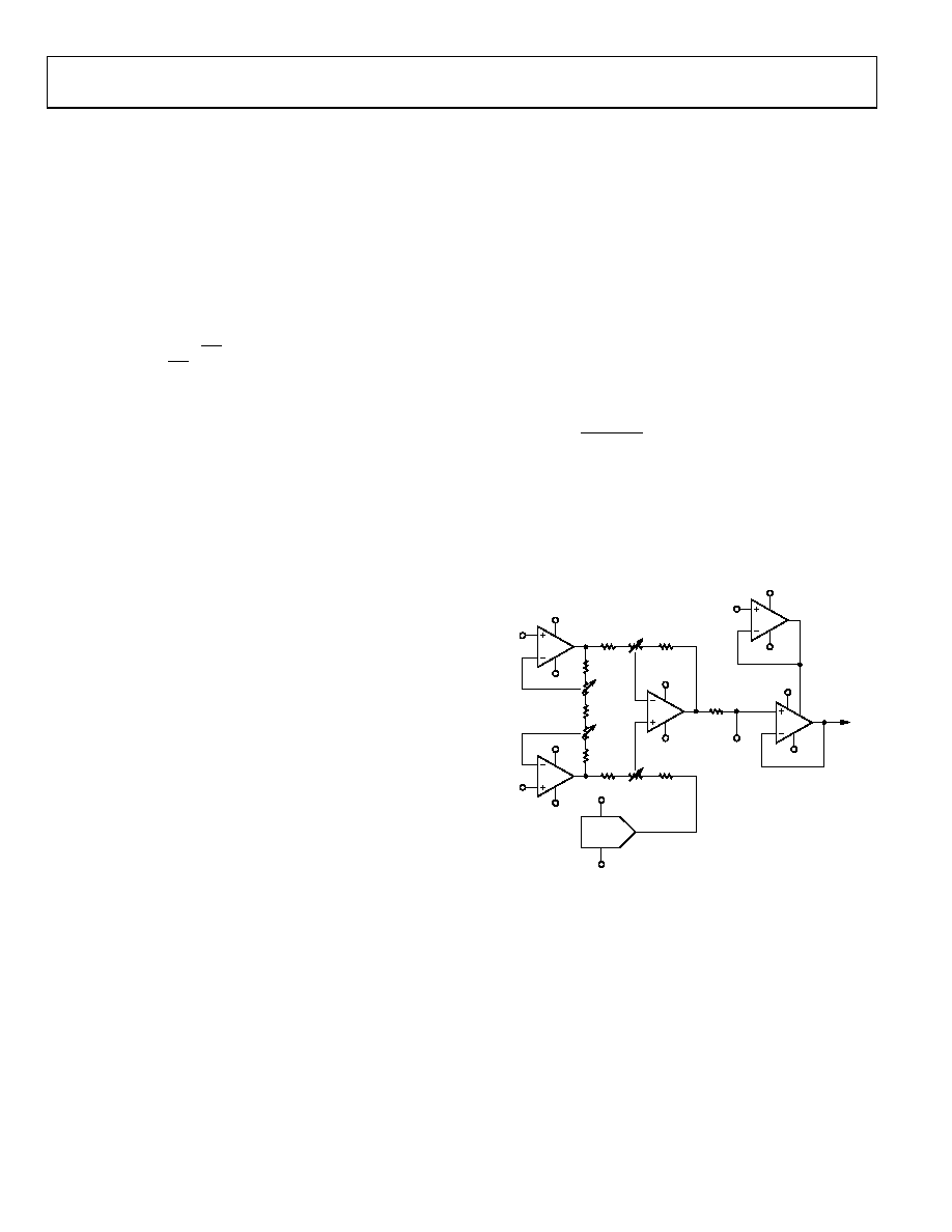
THEORY OF OPERATION
A1, A2, R1, R2, R3, P1, and P2 form the first gain stage of the
differential amplifier. A1 and A2 are auto-zeroed op amps that
minimize input offset errors. P1 and P2 are digital potentiometers,
guaranteed to be monotonic. Programming P1 and P2 allows
the first stage gain to be varied from 4.0 to 6.4 with 7-bit
resolution (see Table 5 and Equation 1), giving a fine gain
adjustment resolution of 0.37%. R1, R2, R3, P1, and P2 each
have a similar temperature coefficient; therefore, the first stage
gain temperature coefficient is lower than 100 ppm/°C.
×
≈
127
4
6.4
4
Code
GAIN1
(1)
A3, R4, R5, R6, R7, P3, and P4 form the second gain stage of
the differential amplifier. A3 is also an auto-zeroed op amp that
minimizes input offset errors. P3 and P4 are digital potentiometers
that allow the second stage gain to be varied from 17.5 to 200 in
eight steps (see Table 6). R4, R5, R6, R7, P3, and P4 each have a
similar temperature coefficient; therefore, the second stage gain
temperature coefficient is lower than 100 ppm/°C.
RF together with an external capacitor, connected between
FILT/DIGOUT and VSS or VDD, form a low-pass filter. The
filtered signal is buffered by A4 to give a low impedance output
at VOUT. RF is nominally 18 kΩ, allowing an 880 Hz low-pass
filter to be implemented by connecting a 10 nF external capacitor
between FILT/DIGOUT and VSS or between FILT/DIGOUT
and VDD. If low-pass filtering is not needed, the FILT/DIGOUT
pin must be left floating.
A5 implements a voltage buffer that provides the positive supply
to A4, the amplifier output buffer. Its function is to limit VOUT
to a maximum value, useful for driving ADCs operating on
supply voltages lower than VDD. The input to A5, VCLAMP,
has a very high input resistance. It should be connected to a
known voltage and not left floating. However, the high input
impedance allows the clamp voltage to be set using a high
impedance source, such as a potential divider. If the maximum
value of VOUT does not need to be limited, VCLAMP should
be connected to VDD.
A4 implements a rail-to-rail input and output unity-gain
voltage buffer. The output stage of A4 is supplied from a
buffered version of VCLAMP instead of VDD, allowing the
positive swing to be limited. The maximum output current is
limited between 5 mA to 10 mA.
An 8-bit DAC is used to generate a variable offset for the
amplifier output. This DAC is guaranteed to be monotonic.
To preserve the ratiometric nature of the input signal, the DAC
references are driven from VSS and VDD, and the DAC output
can swing from VSS (Code 0) to VDD (Code 255). The 8-bit
resolution is equivalent to 0.39% of the difference between
VDD and VSS, for example, 19.5 mV with a 5 V supply. The
DAC output voltage (VDAC) is given approximately by
() VSS
VSS
VDD
Code
VDAC
+
+
≈
256
0.5
(2)
where the temperature coefficient of VDAC is lower than
200 ppm/°C.
The amplifier output voltage (VOUT) is given by
VOUT
= GAIN (VPOS VNEG) + VDAC
(3)
where GAIN is the product of the first and second stage gains.
A3
A2
A4
A5
VDD
DAC
VSS
VDD
VSS
VDD
VSS
VCLAMP
VPOS
VSS
FILT/
DIGOUT
VOUT
A1
VDD
VSS
VNEG
R1
R3
R2
R5
R7
P4
R4
R6
RF
P3
P2
P1
0544
8-
00
1
Figure 47. Functional Schematic
相关PDF资料 |
PDF描述 |
|---|---|
| C22G63S | FUSE INDUST 63A 690V CLASS GG |
| HMTSW-102-07-G-S-240 | CONN HEADER 2POS .100" T/H GOLD |
| SY88343HLMG TR | IC AMP CML LIMITING POST 16MLF |
| C22G80S | FUSE INDUST 80A 500V CLASS GG |
| TMM-103-03-T-S | CONN HEADER 3POS .079" T/H TIN |
相关代理商/技术参数 |
参数描述 |
|---|---|
| AD8556ARZ-REEL7 | 功能描述:IC AMP CHOPPER 2MHZ 10MA 8SOIC RoHS:是 类别:集成电路 (IC) >> Linear - Amplifiers - Instrumentation 系列:DigiTrim® 标准包装:73 系列:Over-The-Top® 放大器类型:通用 电路数:4 输出类型:满摆幅 转换速率:0.07 V/µs 增益带宽积:200kHz -3db带宽:- 电流 - 输入偏压:1nA 电压 - 输入偏移:285µV 电流 - 电源:50µA 电流 - 输出 / 通道:25mA 电压 - 电源,单路/双路(±):2 V ~ 44 V,±1 V ~ 22 V 工作温度:-40°C ~ 85°C 安装类型:表面贴装 封装/外壳:16-WFDFN 裸露焊盘 供应商设备封装:16-DFN-EP(5x3) 包装:管件 |
| AD8556CP-EBZ | 功能描述:AD8556 DigiTrim? Series 1 - Single Channels per IC Chopper (Zero-Drift) Amplifier Evaluation Board 制造商:analog devices inc. 系列:DigiTrim? 零件状态:有效 每 IC 通道数:1 - 单 放大器类型:断路器(零漂移) 输出类型:单端 压摆率:1.2 V/μs -3db 带宽:- 电流 - 输出/通道:10mA 工作温度:-40°C ~ 140°C 电流 - 电源(主 IC):2mA 电压 - 电源,单/双(±):4.5 V ~ 5.5 V 板类型:完全填充 所含物品:板 使用的 IC/零件:AD8556 标准包装:1 |
| AD8556-EVALZ | 制造商:Analog Devices 功能描述:EVALUATION BOARD - Boxed Product (Development Kits) |
| AD8557 | 制造商:AD 制造商全称:Analog Devices 功能描述:Wide Supply Range, Micropower, |
| AD85571 | 制造商:AD 制造商全称:Analog Devices 功能描述:10 MHz, 20 V/レs, G = 1, 10, 100, 1000 i CMOS㈢ Programmable Gain Instrumentation Amplifier |
发布紧急采购,3分钟左右您将得到回复。