- 您现在的位置:买卖IC网 > PDF目录3298 > AD8557ACPZ-REEL (Analog Devices Inc)IC AMP CHOPPER 2MHZ 55MA 16LFCSP PDF资料下载
参数资料
| 型号: | AD8557ACPZ-REEL |
| 厂商: | Analog Devices Inc |
| 文件页数: | 8/24页 |
| 文件大小: | 0K |
| 描述: | IC AMP CHOPPER 2MHZ 55MA 16LFCSP |
| 标准包装: | 5,000 |
| 系列: | DigiTrim® |
| 放大器类型: | 断路器(零漂移) |
| 电路数: | 1 |
| 增益带宽积: | 2MHz |
| 电流 - 输入偏压: | 18nA |
| 电压 - 输入偏移: | 2µV |
| 电流 - 电源: | 1.8mA |
| 电流 - 输出 / 通道: | 55mA |
| 电压 - 电源,单路/双路(±): | 2.7 V ~ 5.5 V |
| 工作温度: | -40°C ~ 125°C |
| 安装类型: | 表面贴装 |
| 封装/外壳: | 16-VQFN 裸露焊盘,CSP |
| 供应商设备封装: | 16-LFCSP-VQ |
| 包装: | 带卷 (TR) |
AD8557
Rev. C | Page 16 of 24
OPEN WIRE FAULT DETECTION
The inputs to A1 and A2, VNEG and VPOS, each have a com-
parator to detect whether VNEG or VPOS exceeds a threshold
voltage, nominally VDD 1.1 V. If VNEG > (VDD 1.1 V) or
VPOS > (VDD 1.1 V), VOUT is clamped to VSS. The output
current limit circuit is disabled in this mode, but the maximum
sink current is approximately 10 mA when VDD = 5 V. The
inputs to A1 and A2, VNEG and VPOS, are also pulled up to
VDD by currents IP1 and IP2. These are both nominally 16 nA
and matched to within 3 nA. If the inputs to A1 or A2 are
accidentally left floating, as with an open wire fault, IP1 and IP2
pull them to VDD, which would cause VOUT to swing to VSS,
allowing this fault to be detected. It is not possible to disable IP1
and IP2, nor the clamping of VOUT to VSS, when VNEG or
VPOS approaches VDD.
SHORTED WIRE FAULT DETECTION
The AD8557 provides fault detection in the case where VPOS,
VNEG, or VCLAMP shorts to VDD and VSS. Figure 46 shows
the voltage regions at VPOS, VNEG, and VCLAMP that trigger
an error condition. When an error condition occurs, the VOUT
pin is shorted to VSS. Table 8 lists the voltage levels shown in
VPOS
VNEG
VSS
VINL
VINH
VDD
VSS
VCLL
VDD
VCLAMP
VSS
VINL
VINH
VDD
ERROR
NORMAL
ERROR
NORMAL
ERROR
NORMAL
06013-
039
Figure 46. Voltage Regions at VPOS, VNEG, and VCLAMP
that Trigger a Fault Condition
Table 8. Typical VINL, VINH, and VCLL Values
(VDD = 5 V)
Voltage
Min (V)
Max (V)
VOUT Condition
VINH
3.9
4.2
Short to VDD fault detection
VINL
0.195
0.55
Short to VSS fault detection
VCLL
1.0
1.2
Short to VSS fault detection
FLOATING VPOS, VNEG, OR VCLAMP FAULT
DETECTION
A floating fault condition at the VPOS, VNEG, or VCLAMP
pins is detected by using a low current to pull a floating input
into an error voltage range, defined in the previous section. In
this way, the VOUT pin is shorted to VSS when a floating input
is detected. Table 9 lists the currents used.
Table 9. Floating Fault Detection at VPOS, VNEG,
and VCLAMP
Pin
Typical Current
Goal of Current
VPOS
16 nA pull-up
Pull VPOS above VINH
VNEG
16 nA pull-up
Pull VNEG above VINH
VCLAMP
0.2 A pull-down
Pull VCLAMP below VCLL
DEVICE PROGRAMMING
Digital Interface
The digital interface allows the first stage gain, second stage
gain, and output offset to be adjusted and allows desired values
for these parameters to be permanently stored by selectively
blowing polysilicon fuses. To minimize pin count and board
space, a single-wire digital interface is used. The digital input
pin, DIGIN, has hysteresis to minimize the possibility of
inadvertent triggering with slow signals. It also has a pull-down
current sink to allow it to be left floating when programming is
not being performed. The pull-down ensures inactive status of
the digital input by forcing a dc low voltage on DIGIN.
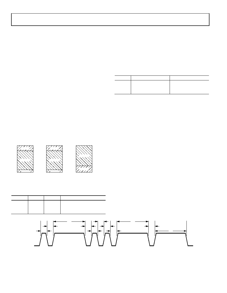
A short pulse at DIGIN from low to high and back to low again,
such as between 50 ns and 10 s long, loads a 0 into a shift
register. A long pulse at DIGIN, such as 50 s or longer, loads a
1 into the shift register. The time between pulses should be at
least 10 s. Assuming VSS = 0 V, voltages at DIGIN between
VSS and 0.2 × VDD are recognized as a low, and voltages at
DIGIN between 0.8 × VDD and VDD are recognized as a high.
A timing diagram example, Figure 47, shows the waveform for
entering Code 010011 into the shift register.
CODE
0
1
0
1
WAVEFORM
tW0
tWS
tW0
tWS
tW0
tWS
tW1
06013-
040
Figure 47. Timing Diagram for Code 010011
相关PDF资料 |
PDF描述 |
|---|---|
| ADA4091-2ACPZ-RL | IC OPAMP GP R-R 1.27MHZ 8LFCSP |
| AD706JRZ-REEL | IC OPAMP GP DUAL PREC 15MA 8SOIC |
| LTC6247ITS8#TRMPBF | IC OPAMP RRIO 180MHZ DL TSOT23-8 |
| LTC6247IKC#TRMPBF | IC OPAMP RRIO 180MHZ DL 8UTDFN |
| 0713085492 | CONN HEADER BKWY SMD TIN 92POS |
相关代理商/技术参数 |
参数描述 |
|---|---|
| AD8557ACPZ-REEL7 | 功能描述:IC AMP CHOPPER 2MHZ 55MA 16LFCSP RoHS:是 类别:集成电路 (IC) >> Linear - Amplifiers - Instrumentation 系列:DigiTrim® 产品培训模块:Differential Circuit Design Techniques for Communication Applications 标准包装:1 系列:- 放大器类型:RF/IF 差分 电路数:1 输出类型:差分 转换速率:9800 V/µs 增益带宽积:- -3db带宽:2.9GHz 电流 - 输入偏压:3µA 电压 - 输入偏移:- 电流 - 电源:40mA 电流 - 输出 / 通道:- 电压 - 电源,单路/双路(±):3 V ~ 3.6 V 工作温度:-40°C ~ 85°C 安装类型:表面贴装 封装/外壳:16-VQFN 裸露焊盘,CSP 供应商设备封装:16-LFCSP-VQ 包装:剪切带 (CT) 产品目录页面:551 (CN2011-ZH PDF) 其它名称:ADL5561ACPZ-R7CT |
| AD8557ARZ | 功能描述:IC AMP CHOPPER 2MHZ 55MA 8SOIC RoHS:是 类别:集成电路 (IC) >> Linear - Amplifiers - Instrumentation 系列:DigiTrim® 标准包装:2,500 系列:- 放大器类型:通用 电路数:4 输出类型:- 转换速率:0.6 V/µs 增益带宽积:1MHz -3db带宽:- 电流 - 输入偏压:45nA 电压 - 输入偏移:2000µV 电流 - 电源:1.4mA 电流 - 输出 / 通道:40mA 电压 - 电源,单路/双路(±):3 V ~ 32 V,±1.5 V ~ 16 V 工作温度:0°C ~ 70°C 安装类型:表面贴装 封装/外壳:14-TSSOP(0.173",4.40mm 宽) 供应商设备封装:14-TSSOP 包装:带卷 (TR) 其它名称:LM324ADTBR2G-NDLM324ADTBR2GOSTR |
| AD8557ARZ-REEL | 功能描述:IC AMP CHOPPER 2MHZ 55MA 8SOIC RoHS:是 类别:集成电路 (IC) >> Linear - Amplifiers - Instrumentation 系列:DigiTrim® 其它有关文件:Automotive Product Guide 产品培训模块:Lead (SnPb) Finish for COTS Obsolescence Mitigation Program 标准包装:1 系列:- 放大器类型:通用 电路数:1 输出类型:满摆幅 转换速率:3 V/µs 增益带宽积:10MHz -3db带宽:- 电流 - 输入偏压:1pA 电压 - 输入偏移:70µV 电流 - 电源:2.5mA 电流 - 输出 / 通道:48mA 电压 - 电源,单路/双路(±):2.7 V ~ 5.5 V,±1.35 V ~ 2.75 V 工作温度:-40°C ~ 125°C 安装类型:表面贴装 封装/外壳:SOT-23-6 供应商设备封装:SOT-6 包装:Digi-Reel® 其它名称:MAX4475AUT#TG16DKR |
| AD8557ARZ-REEL7 | 功能描述:IC AMP CHOPPER 2MHZ 55MA 8SOIC RoHS:是 类别:集成电路 (IC) >> Linear - Amplifiers - Instrumentation 系列:DigiTrim® 产品培训模块:Lead (SnPb) Finish for COTS Obsolescence Mitigation Program 标准包装:1 系列:- 放大器类型:电流检测 电路数:1 输出类型:- 转换速率:- 增益带宽积:125kHz -3db带宽:- 电流 - 输入偏压:- 电压 - 输入偏移:100µV 电流 - 电源:1.1µA 电流 - 输出 / 通道:- 电压 - 电源,单路/双路(±):- 工作温度:-40°C ~ 85°C 安装类型:表面贴装 封装/外壳:4-WFBGA,CSPBGA 供应商设备封装:4-UCSP(2x2) 包装:剪切带 (CT) 其它名称:MAX9634WERS+TCT |
| AD8558WACPZ-R2 | 功能描述:IC OPAMP CHOPPER 2MHZ 16LFCSP 制造商:analog devices inc. 系列:* 零件状态:上次购买时间 标准包装:1 |
发布紧急采购,3分钟左右您将得到回复。