- 您现在的位置:买卖IC网 > PDF目录10796 > AD8561ARZ-REEL7 (Analog Devices Inc)IC COMP 7NS ULTRA-FAST 8-SOIC PDF资料下载
参数资料
| 型号: | AD8561ARZ-REEL7 |
| 厂商: | Analog Devices Inc |
| 文件页数: | 7/12页 |
| 文件大小: | 0K |
| 描述: | IC COMP 7NS ULTRA-FAST 8-SOIC |
| 标准包装: | 1 |
| 类型: | 通用 |
| 元件数: | 1 |
| 输出类型: | CMOS,补充型,TTL |
| 电压 - 电源,单路/双路(±): | 3 V ~ 10 V,±1.5 V ~ 5 V |
| 电压 - 输入偏移(最小值): | 7mV @ 5V |
| 电流 - 输入偏压(最小值): | 6µA @ 5V |
| 电流 - 静态(最大值): | 6mA,3.3mA,5.5mA |
| CMRR, PSRR(标准): | 85dB CMRR,65dB PSRR |
| 传输延迟(最大): | 9.8ns |
| 工作温度: | -40°C ~ 85°C |
| 封装/外壳: | 8-SOIC(0.154",3.90mm 宽) |
| 安装类型: | 表面贴装 |
| 包装: | 标准包装 |
| 产品目录页面: | 764 (CN2011-ZH PDF) |
| 其它名称: | AD8561ARZ-REEL7DKR |
–4–
AD8561–SPECIFICATIONS
CAUTION
ESD (electrostatic discharge) sensitive device. Electrostatic charges as high as 4000 V readily
accumulate on the human body and test equipment and can discharge without detection.
Although the AD8561 features proprietary ESD protection circuitry, permanent damage may
occur on devices subjected to high energy electrostatic discharges. Therefore, proper ESD
precautions are recommended to avoid performance degradation or loss of functionality.
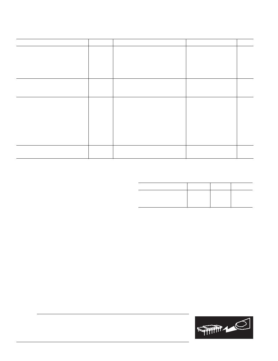
ELECTRICAL SPECIFICATIONS
Parameter
Symbol
Conditions
Min
Typ
Max
Units
INPUT CHARACTERISTICS
Offset Voltage
VOS
7mV
Input Bias Current
IB
VCM = 0 V
–6
–3.0
μA
IB
–40
°C ≤ TA ≤ +85°C–7
–4
μA
Input Common-Mode Voltage Range
VCM
0
+1.5
V
Common-Mode Rejection Ratio
CMRR
0.1 V
≤ VCM ≤ 1.5 V
60
dB
OUTPUT CHARACTERISTICS
Output High Voltage
VOH
IOH = –3.2 mA, VIN > 250 mV
1.21
V
Output Low Voltage
VOL
IOL = +3.2 mA, VIN > 250 mV
0.3
V
POWER SUPPLY
Power Supply Rejection Ratio
PSRR
+2.7 V
≤ V
CC, VEE
≤ +6 V
40
dB
Supply Currents
VO = 0 V, RL =
∞
V+ Supply Current
I+
4.0
4.5
mA
–40
°C ≤ T
A
≤ +85°C
5.5
mA
Ground Supply Current
IGND
1.6
2.5
mA
–40
°C ≤ T
A
≤ +85°C
3.0
mA
V– Supply Current
I–
2.4
3.3
mA
–40
°C ≤ T
A
≤ +85°C
3.8
mA
DYNAMIC PERFORMANCE
Propagation Delay
tP
100 mV Step with 20 mV Overdrive
2
8.5
9.8
ns
NOTES
1Output high voltage without pull-up resistor. It may be useful to have a pull-up resistor to V+ for 3 V operation.
2Guaranteed by design.
Specifications subject to change without notice.
(@ V+ = +3.0 V, V– = VGND = 0 V, TA = +25 C unless otherwise noted)
ABSOLUTE MAXIMUM RATINGS
Total Analog Supply Voltage . . . . . . . . . . . . . . . . . . . . . +14 V
Digital Supply Voltage . . . . . . . . . . . . . . . . . . . . . . . . . . +14 V
Analog Positive Supply–Digital Positive Supply . . . . . –600 mV
Input Voltage
1 . . . . . . . . . . . . . . . . . . . . . . . . . . . . . . . . .
±7 V
Differential Input Voltage . . . . . . . . . . . . . . . . . . . . . . . .
±8 V
Output Short-Circuit Duration to GND . . . . . . . . . Indefinite
Storage Temperature Range
N, R, RU Package . . . . . . . . . . . . . . . . . . –65
°C to +150°C
Operating Temperature Range . . . . . . . . . . . –40
°C to +85°C
Junction Temperature Range
N, R, RU Package . . . . . . . . . . . . . . . . . . –65
°C to +150°C
Lead Temperature Range (Soldering, 10 sec) . . . . . . . +3 0
°C
Package Type
JA
2
JC
Units
8-Lead Plastic DIP (N)
103
43
°C/W
8-Lead SO (R)
158
43
°C/W
8-Lead TSSOP
240
43
°C/W
NOTES
1The analog input voltage is equal to
±7 V or the analog supply voltage, whichever
is less.
2
θ
JA is specified for the worst case conditions, i.e.,
θ
JA is specified for device in socket
for P-DIP and
θ
JA is specified for device soldered in circuit board for SOIC and
TSSOP packages.
WARNING!
ESD SENSITIVE DEVICE
Rev. B
5
相关PDF资料 |
PDF描述 |
|---|---|
| LT1780CSW#PBF | IC DVR/RCVR 5V RS232 DUAL 18SOIC |
| VE-JNL-MW-F4 | CONVERTER MOD DC/DC 28V 100W |
| LTC2862IDD-2#PBF | IC TRANSCEIVER RS485 8-DFN |
| VI-JTL-MY-S | CONVERTER MOD DC/DC 28V 50W |
| LTC1386CS#PBF | IC TXRX 3.3V EIA/TIA-562 16-SOIC |
相关代理商/技术参数 |
参数描述 |
|---|---|
| AD8563 | 制造商:AD 制造商全称:Analog Devices 功能描述:1.8 V to 5 V Auto-Zero, In-Amp with Shutdown |
| AD8563ARMZ-R2 | 制造商:AD 制造商全称:Analog Devices 功能描述:1.8 V to 5 V Auto-Zero, In-Amp with Shutdown |
| AD8563ARMZ-REEL | 制造商:AD 制造商全称:Analog Devices 功能描述:1.8 V to 5 V Auto-Zero, In-Amp with Shutdown |
| AD8564 | 制造商:AD 制造商全称:Analog Devices 功能描述:Quad 7 ns Single Supply Comparator |
| AD8564_07 | 制造商:AD 制造商全称:Analog Devices 功能描述:Quad 7 ns Single Supply Comparator |
发布紧急采购,3分钟左右您将得到回复。