- 您现在的位置:买卖IC网 > PDF目录5452 > AD8566ARMZ-REEL (Analog Devices Inc)IC OPAMP GP R-R 5MHZ DUAL 8MSOP PDF资料下载
参数资料
| 型号: | AD8566ARMZ-REEL |
| 厂商: | Analog Devices Inc |
| 文件页数: | 3/16页 |
| 文件大小: | 0K |
| 描述: | IC OPAMP GP R-R 5MHZ DUAL 8MSOP |
| 标准包装: | 3,000 |
| 放大器类型: | 通用 |
| 电路数: | 2 |
| 输出类型: | 满摆幅 |
| 转换速率: | 6 V/µs |
| 增益带宽积: | 5MHz |
| 电流 - 输入偏压: | 80nA |
| 电压 - 输入偏移: | 2000µV |
| 电流 - 电源: | 700µA |
| 电流 - 输出 / 通道: | 35mA |
| 电压 - 电源,单路/双路(±): | 4.5 V ~ 16 V |
| 工作温度: | -40°C ~ 85°C |
| 安装类型: | 表面贴装 |
| 封装/外壳: | 8-TSSOP,8-MSOP(0.118",3.00mm 宽) |
| 供应商设备封装: | 8-MSOP |
| 包装: | 带卷 (TR) |
AD8565/AD8566/AD8567
Rev. G | Page 11 of 16
TOTAL HARMONIC DISTORTION + NOISE (THD + N)
The AD8565/AD8566/AD8567 feature low total harmonic dis-
tortion. Figure 31 shows THD + N vs. frequency. The THD + N
over the entire supply range is below 0.008%. When the device
is powered from a 16 V supply, the THD + N stays below
0.003%. Figure 31 shows the AD8566 in a unity noninverting
configuration.
FREQUENCY (Hz)
20
T
HD+
N
(
%)
100
10
1
0.01
0.1
1k
10k
30k
VS = ±2.5V
VS = ±8V
01909-
031
Figure 31. THD + N vs. Frequency
SHORT-CIRCUIT OUTPUT CONDITIONS
The AD8565/AD8566/AD8567 do not have internal short-
circuit protection circuitry. As a precautionary measure, it is
recommended not to short the output directly to the positive
power supply or to ground.
It is not recommended to operate the AD8565/AD8566/AD8567
with more than 35 mA of continuous output current. The
output current can be limited by placing a series resistor at the
output of the amplifier whose value can be derived using
mA
35
S
X
V
R ≥
For a 5 V single-supply operation, RX should have a minimum
value of 143 .
LCD PANEL APPLICATIONS
The AD8565/AD8566/AD8567 amplifier is designed for LCD
panel applications or applications where large capacitive load
drive is required. It can instantaneously source/sink greater than
250 mA of current. At unity gain, it can drive 1 F without
compensation. This makes the AD8565/AD8566/AD8567 ideal
for LCD VCOM driver applications.
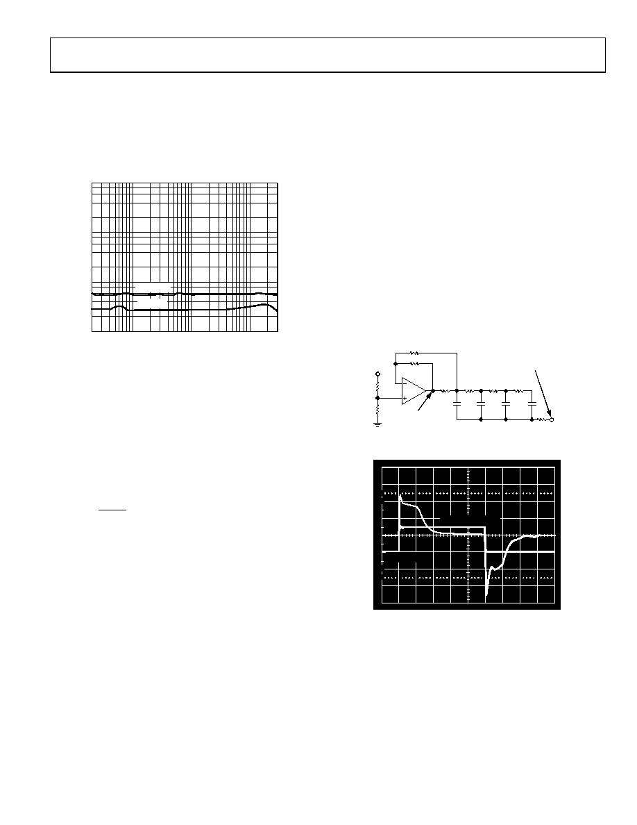
To evaluate the performance of the AD8565/AD8566/AD8567,
a test circuit was developed to simulate the VCOM driver
application for an LCD panel. Figure 32 shows the test circuit.
Series capacitors and resistors connected to the output of the op
amp represent the load of the LCD panel. The 300 and 3 k
feedback resistors are used to improve settling time. This test
circuit simulates the worst-case scenario for a VCOM. It drives a
represented load that is connected to a signal switched symmet-
rically around VCOM.
Figure 33 shows a scope photo of the instantaneous output peak
current capability of the AD8565/AD8566/AD8567.
INPUT 0V TO 8V
SQUARE WAVE WITH
15.6s PULSE WIDTH
300
3k
10
10
10
10
10nF
MEASURE
CURRENT
4V
8V
10
TO 20
01909-
032
Figure 32. VCOM Test Circuit with Supply Voltage at 16 V
TIME (2s/DIV)
01909-
033
CH 2 = 100mA/DIV
CH 1 = 5V/DIV
10
0%
100
90
Figure 33. Scope Photo of the VCOM Instantaneous Peak Current
相关PDF资料 |
PDF描述 |
|---|---|
| AD8646WARZ-R7 | IC OPAMP GP R-R 24MHZ DUAL 8SOIC |
| BK/FLF-40 | FUSE 40A AUTO |
| 51866-025 | POWERBLADE R/A REC |
| MDL-V-20-R | FUSE 20A 32V T-LAG AXIAL |
| W51-A152A1-5 | CIRCUIT BRKR THERMAL 5A BLK |
相关代理商/技术参数 |
参数描述 |
|---|---|
| AD8566WARMZ-REEL | 制造商:Analog Devices 功能描述: |
| AD8567 | 制造商:AD 制造商全称:Analog Devices 功能描述:16 V Rail-to-Rail Operational Amplifiers |
| AD8567ACP | 制造商:AD 制造商全称:Analog Devices 功能描述:16 V Rail-to-Rail Operational Amplifiers |
| AD8567ACP-R2 | 制造商:Analog Devices 功能描述:OP Amp Quad GP R-R I/O 16V 16-Pin LFCSP EP T/R 制造商:Rochester Electronics LLC 功能描述:QUAD 16V 35MA CBCMOS AMPLIFIER - Bulk |
| AD8567ACP-REEL | 制造商:Analog Devices 功能描述: |
发布紧急采购,3分钟左右您将得到回复。