参数资料
| 型号: | AD8567ARUZ-REEL |
| 厂商: | Analog Devices Inc |
| 文件页数: | 16/16页 |
| 文件大小: | 0K |
| 描述: | IC OPAMP GP R-R 5MHZ 14TSSOP |
| 标准包装: | 2,500 |
| 放大器类型: | 通用 |
| 电路数: | 4 |
| 输出类型: | 满摆幅 |
| 转换速率: | 6 V/µs |
| 增益带宽积: | 5MHz |
| 电流 - 输入偏压: | 80nA |
| 电压 - 输入偏移: | 2000µV |
| 电流 - 电源: | 700µA |
| 电流 - 输出 / 通道: | 35mA |
| 电压 - 电源,单路/双路(±): | 4.5 V ~ 16 V |
| 工作温度: | -40°C ~ 85°C |
| 安装类型: | 表面贴装 |
| 封装/外壳: | 14-TSSOP(0.173",4.40mm 宽) |
| 供应商设备封装: | 14-TSSOP |
| 包装: | 带卷 (TR) |
AD8565/AD8566/AD8567
Rev. G | Page 9 of 16
THEORY OF OPERATION
The AD8565/AD8566/AD8567 are designed to drive large
capacitive loads in LCD applications. They have high output
current drive and rail-to-rail input/output operation and are
powered from a single 16 V supply. They are also intended for
other applications where low distortion and high output current
drive are needed.
Figure 28 shows a simplified equivalent circuit for the AD8565/
AD8566/AD8567. The rail-to-rail bipolar input stage is com-
posed of two PNP differential pairs, Q4 to Q5 and Q10 to Q11,
operating in series with diode protection networks, D1 to D2.
Diode network D1 to D2 serves as protection against large
transients for Q4 to Q5 to accommodate rail-to-rail input swing.
D5 to D6 protect Q10 to Q11 against Zenering. In normal oper-
ation, Q10 to Q11 are off, and their input stage is buffered from
the operational amplifier inputs by Q6 to D3 and Q8 to D4.
Operation of the input stage is best understood as a function of
applied common-mode voltage: when the inputs of the AD8565/
AD8566/AD8567 are biased midway between the supplies, the
differential signal path gain is controlled by resistive loads Q4 to
Q5 (via R9, R10). As the input common-mode level is reduced
toward the negative supply (VNEG or GND), the input transistor
current sources, I1 and I2, are forced into saturation, thereby
forcing the Q6 to D3 and Q8 to D4 networks into cutoff.
However, Q4 to Q5 remain active, providing input stage gain.
Inversely, when common-mode input voltage is increased
toward the positive supply, Q4 to Q5 are driven into cutoff, Q3
is driven into saturation, and Q4 becomes active, providing bias
to the Q10 to Q11 differential pair. The point at which the Q10 to
Q11 differential pair becomes active is approximately equal to
(VPOS 1 V).
R1
R4
R3
D2
D1
Q4
Q3
BIAS LINE
V–
D4
D3
Q5
Q4
Q10
Q11
C1
C2
D5
D6
Q8
Q6
R10
R9
FOLDED
CASCADE
V+
I2
I1
VNEG
VPOS
R5
R6
01909-
028
Figure 28. AD8565/AD8566/AD8567 Equivalent Input Circuit
The benefit of this type of input stage is low bias current. The
input bias current is the sum of base currents of Q4 to Q5 and
Q6 to Q8 over the range from (VNEG + 1 V) to (VPOS 1 V).
Outside this range, the input bias current is dominated by the
sum of base currents of Q10 to Q11 for input signals close to
VNEG and of Q6 to Q8 (Q10 to Q11) for signals close to VPOS.
From this type of design, the input bias current of the AD8565/
AD8566/AD8567 not only exhibits different amplitude but also
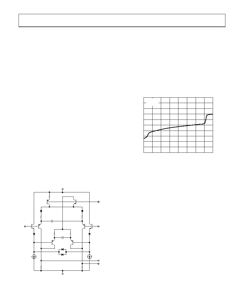
exhibits different polarities. Figure 29 provides the characteris-
tics of the input bias current vs. the common-mode voltage. It is
important to keep in mind that the source impedances driving
the inputs are balanced for optimum dc and ac performance.
INPUT COMMON-MODE VOLTAGE (V)
0
2
INP
UT
BI
AS
CURRE
NT
(
n
A)
1000
–1000
800
200
–200
–600
–800
600
400
0
–400
4
6
8
10
12
14
16
VS = 16V
TA = 25°C
01909-
029
Figure 29. AD8565/AD8566/AD8567 Input Bias Current vs.
Common-Mode Voltage
To achieve rail-to-rail output performance, the AD8565/
AD8566/AD8567 design uses a complementary common-
source (or gmRL) output. This con-figuration allows output
voltages to approach the power supply rails, particularly if the
output transistors are allowed to enter the triode region on
extremes of signal swing, which are limited by VGS, the
transistor sizes, and output load current. In addition, this type
of output stage exhibits voltage gain in an open-loop gain
configuration. The amount of gain depends on the total load
resistance at the output of the AD8565/AD8566/AD8567.
INPUT OVERVOLTAGE PROTECTION
As with any semiconductor device, whenever the input exceeds
either supply voltages, attention needs to be paid to the input
overvoltage characteristics. As an overvoltage occurs, the amplifier
could be damaged, depending on the voltage level and the
magnitude of the fault current. When the input voltage exceeds
either supply by more than 0.6 V, internal positive-negative (pn)
junctions allow current to flow from the input to the supplies.
相关PDF资料 |
PDF描述 |
|---|---|
| TSW-127-06-T-D | CONN HEADER 54POS .100" DL TIN |
| LTC6087CMS8#TRPBF | IC AMP DUAL CMOS R-R 8-MSOP |
| TSW-128-06-T-D | CONN HEADER 56POS .100" DL TIN |
| LTC6087CDD#TRPBF | IC AMP DUAL CMOS R-R 10-DFN |
| TSW-129-06-T-D | CONN HEADER 58POS .100" DL TIN |
相关代理商/技术参数 |
参数描述 |
|---|---|
| AD8568 | 制造商:AD 制造商全称:Analog Devices 功能描述:16 V Rail-to-Rail Buffer Amplifiers |
| AD8568_03 | 制造商:AD 制造商全称:Analog Devices 功能描述:16 V Rail-to-Rail Buffer Amplifiers |
| AD8568ART | 制造商:AD 制造商全称:Analog Devices 功能描述:16 V Rail-to-Rail Buffer Amplifiers |
| AD8568ART-R2 | 制造商:Analog Devices 功能描述:OP Amp Dual GP R-R I/O 16V 6-Pin SOT-23 T/R 制造商:Analog Devices 功能描述:OP AMP DUAL GP R-R I/O 16V 6PIN SOT-23 - Tape and Reel 制造商:Rochester Electronics LLC 功能描述:DUAL 16V 35MA CBCMOS BUFFER - Bulk |
| AD8568ART-REEL | 制造商:Analog Devices 功能描述: |
发布紧急采购,3分钟左右您将得到回复。