参数资料
| 型号: | AD8571ARMZ |
| 厂商: | Analog Devices Inc |
| 文件页数: | 8/24页 |
| 文件大小: | 0K |
| 描述: | IC OPAMP CHOPPER R-R 30MA 8MSOP |
| 标准包装: | 50 |
| 放大器类型: | 断路器(零漂移) |
| 电路数: | 1 |
| 输出类型: | 满摆幅 |
| 转换速率: | 0.4 V/µs |
| 增益带宽积: | 1.5MHz |
| 电流 - 输入偏压: | 10pA |
| 电压 - 输入偏移: | 1µV |
| 电流 - 电源: | 850µA |
| 电流 - 输出 / 通道: | 30mA |
| 电压 - 电源,单路/双路(±): | 2.7 V ~ 5.5 V |
| 工作温度: | -40°C ~ 125°C |
| 安装类型: | 表面贴装 |
| 封装/外壳: | 8-TSSOP,8-MSOP(0.118",3.00mm 宽) |
| 供应商设备封装: | 8-MSOP |
| 包装: | 管件 |
AD8571/AD8572/AD8574
Rev. E | Page 16 of 24
Therefore,
A
OSB
OSA
EFF
OS
B
V
+
≈
,
(14)
Thus, the offset voltages of both the primary and nulling
amplifiers are reduced by the gain factor BA, which takes a typical
input offset voltage from several millivolts down to an effective
input offset voltage of submicrovolts. This autocorrection scheme
makes the AD857x family of amplifiers extremely precise.
HIGH GAIN, CMRR, AND PSRR
Common-mode and power supply rejection are indications of the
amount of offset voltage an amplifier has as a result of a change in
its input common-mode or power supply voltages. As shown in
the Amplification Phase section, the autocorrection architecture
of the AD857x allows it to effectively minimize offset voltages.
The technique also corrects for offset errors caused by common-
mode voltage swings and power supply variations, which results
in superb CMRR and PSRR figures in excess of 130 dB. Because
the autocorrection occurs continuously, these figures can be
maintained across the temperature range of the device (40°C
to +125°C).
MAXIMIZING PERFORMANCE THROUGH PROPER
LAYOUT
To achieve the maximum performance of the extremely high
input impedance and low offset voltage of the AD857x, care
should be taken in the circuit board layout. The PCB surface
must remain clean and free of moisture to avoid leakage currents
between adjacent traces. Surface coating of the circuit board
reduces surface moisture and provides a humidity barrier, reducing
parasitic resistance on the board. The use of guard rings around
the amplifier inputs further reduces leakage currents. Figure 52
shows how the guard ring should be configured, and Figure 53
shows the top view of how a surface-mount layout can be
arranged. The guard ring does not need to be a specific width,
but it should form a continuous loop around both inputs. By
setting the guard ring voltage equal to the voltage at the non-
inverting input, parasitic capacitance is minimized as well. For
further reduction of leakage currents, components can be mounted
to the PCB using Teflon standoff insulators.
VOUT
VIN
AD8572
VIN
AD8572
V
IN
AD8572
0
110
4-
05
2
Figure 52. Guard Ring Layout and Connections to
Reduce PCB Leakage Currents
V–
V+
VREF
VIN1
VIN2
GUARD
RING
R1
R2
R1
AD8572
GUARD
RING
01
10
4-
0
53
Figure 53. Top View of AD8572 SOIC Layout with Guard Rings
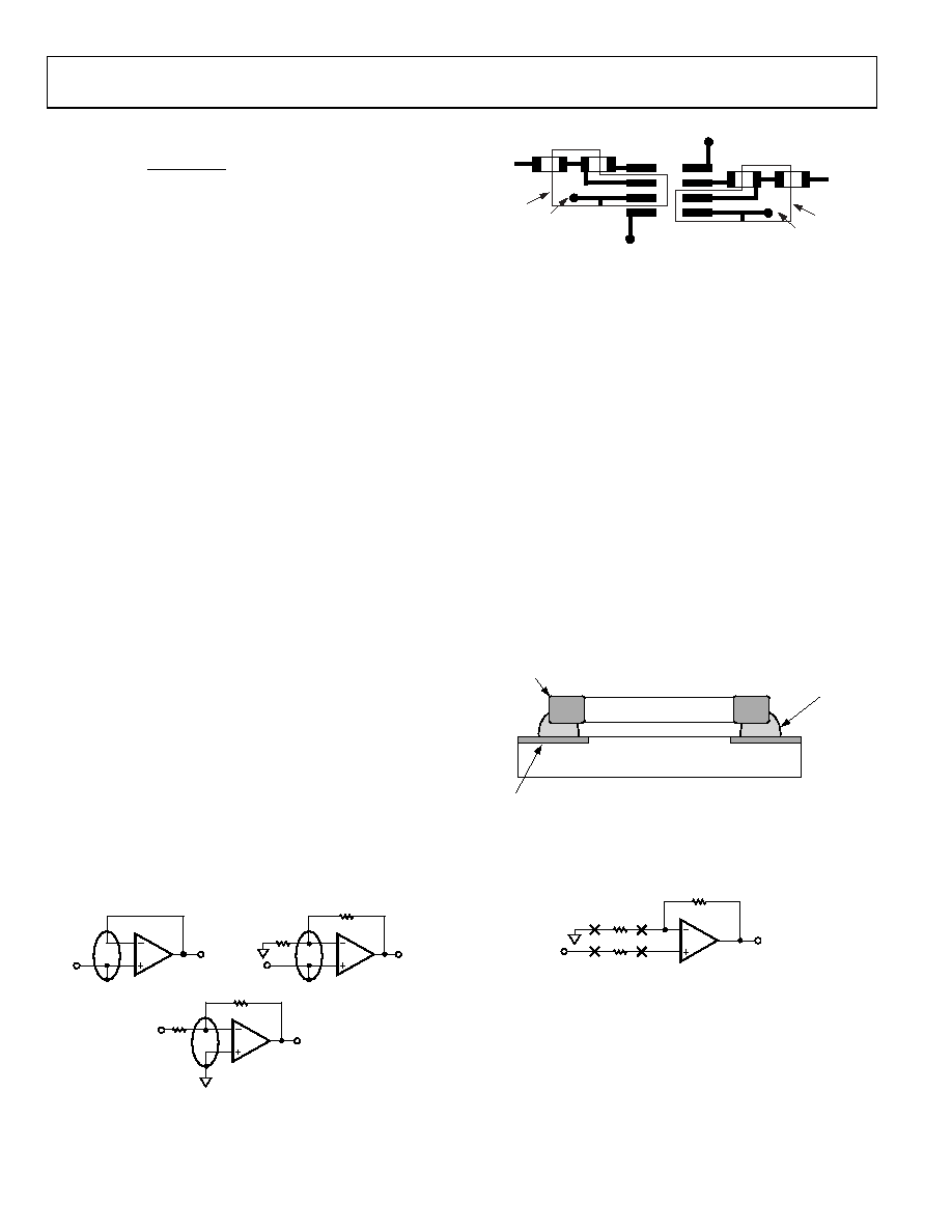
Other potential sources of offset error are thermoelectric
voltages on the circuit board. This voltage, also called Seebeck
voltage, occurs at the junction of two dissimilar metals and is
proportional to the junction temperature. The most common
metallic junctions on a circuit board are solder-to-board trace
and solder-to-component lead. Figure 54 shows a cross-section
view of the thermal voltage error sources. When the temperature
of the PCB at one end of the component (TA1) differs from the
temperature at the other end (TA2), the Seebeck voltages are not
equal, resulting in a thermal voltage error.
This thermocouple error can be reduced by using dummy
components to match the thermoelectric error source. Placing
the dummy component as close as possible to its partner ensures
that both Seebeck voltages are equal, thus canceling the thermo-
couple error. Maintaining a constant ambient temperature on the
circuit board further reduces this error. The use of a ground
plane helps distribute heat throughout the board and also
reduces EMI noise pickup.
SURFACE MOUNT
COMPONENT
LEAD
SOLDER
PC BOARD
COPPER
TRACE
TA2
IF TA1 ≠ TA2, THEN
VTS1 + VSC1 ≠ VTS2 + VSC2
TA1
VSC1
VTS1
+
–
+
–
VSC2
VTS2
+
–
01
10
4-
05
4
Figure 54. Mismatch in Seebeck Voltages Causes a Thermoelectric Voltage Error
RS SHOULD BE PLACED IN CLOSE PROXIMITY AND
ALIGNMENT TO R1 TO BALANCE SEEBECK VOLTAGES
VOUT
VIN
AD8571/AD8572/
AD8574
AV = 1 + (RF /R1)
RF
RS = R1
R1
0
110
4-
0
55
Figure 55. Using Dummy Components to Cancel Thermoelectric Voltage Errors
相关PDF资料 |
PDF描述 |
|---|---|
| 0459844222 | CONN RCPT R/A 4PWR 16SGL 2.36MM |
| 2070.0016.11 | FUSE OSU 250V 1A |
| LTC6101HVACS5#TRPBF | IC AMP CURRENT SENSE TSOT23-5 |
| 0459844213 | CONN RCPT R/A 4PWR 12SGL 1.57MM |
| 0459844212 | CONN RCPT R/A 4PWR 12SGL 2.36MM |
相关代理商/技术参数 |
参数描述 |
|---|---|
| AD8571ARMZ-R2 | 制造商:Analog Devices 功能描述:SP Amp Chopper Stabilization Single R-R I/O 5V 8-Pin MSOP T/R |
| AD8571ARMZ-REEL | 功能描述:IC OPAMP CHOPPER R-R 30MA 8MSOP RoHS:是 类别:集成电路 (IC) >> Linear - Amplifiers - Instrumentation 系列:- 产品培训模块:Differential Circuit Design Techniques for Communication Applications 标准包装:1 系列:- 放大器类型:RF/IF 差分 电路数:1 输出类型:差分 转换速率:9800 V/µs 增益带宽积:- -3db带宽:2.9GHz 电流 - 输入偏压:3µA 电压 - 输入偏移:- 电流 - 电源:40mA 电流 - 输出 / 通道:- 电压 - 电源,单路/双路(±):3 V ~ 3.6 V 工作温度:-40°C ~ 85°C 安装类型:表面贴装 封装/外壳:16-VQFN 裸露焊盘,CSP 供应商设备封装:16-LFCSP-VQ 包装:剪切带 (CT) 产品目录页面:551 (CN2011-ZH PDF) 其它名称:ADL5561ACPZ-R7CT |
| AD8571AR-REEL | 制造商:Analog Devices 功能描述:SP Amp Chopper Stabilization Single R-R I/O 5V 8-Pin SOIC N T/R |
| AD8571AR-REEL7 | 制造商:Analog Devices 功能描述:SP Amp Chopper Stabilization Single R-R I/O 5V 8-Pin SOIC N T/R 制造商:Rochester Electronics LLC 功能描述:SINGLE PRECISION RAIL-RAIL CHOPPER OPAMP - Tape and Reel |
| AD8571ARZ | 功能描述:IC OPAMP CHOPPER R-R 30MA 8SOIC RoHS:是 类别:集成电路 (IC) >> Linear - Amplifiers - Instrumentation 系列:- 产品培训模块:Differential Circuit Design Techniques for Communication Applications 标准包装:1 系列:- 放大器类型:RF/IF 差分 电路数:1 输出类型:差分 转换速率:9800 V/µs 增益带宽积:- -3db带宽:2.9GHz 电流 - 输入偏压:3µA 电压 - 输入偏移:- 电流 - 电源:40mA 电流 - 输出 / 通道:- 电压 - 电源,单路/双路(±):3 V ~ 3.6 V 工作温度:-40°C ~ 85°C 安装类型:表面贴装 封装/外壳:16-VQFN 裸露焊盘,CSP 供应商设备封装:16-LFCSP-VQ 包装:剪切带 (CT) 产品目录页面:551 (CN2011-ZH PDF) 其它名称:ADL5561ACPZ-R7CT |
发布紧急采购,3分钟左右您将得到回复。