参数资料
| 型号: | AD8594ARZ |
| 厂商: | Analog Devices Inc |
| 文件页数: | 3/16页 |
| 文件大小: | 0K |
| 描述: | IC OPAMP GP R-R CMOS 3MHZ 16SOIC |
| 产品变化通告: | Product Discontinuance 27/Oct/2011 |
| 标准包装: | 48 |
| 放大器类型: | 通用 |
| 电路数: | 4 |
| 输出类型: | 满摆幅 |
| 转换速率: | 5 V/µs |
| 增益带宽积: | 3MHz |
| 电流 - 输入偏压: | 5pA |
| 电压 - 输入偏移: | 2000µV |
| 电流 - 电源: | 1.25mA |
| 电流 - 输出 / 通道: | 250mA |
| 电压 - 电源,单路/双路(±): | 2.5 V ~ 6 V,±1.25 V ~ 3 V |
| 工作温度: | -40°C ~ 85°C |
| 安装类型: | 表面贴装 |
| 封装/外壳: | 16-SOIC(0.154",3.90mm 宽) |
| 供应商设备封装: | 16-SOIC |
| 包装: | 管件 |
| 产品目录页面: | 767 (CN2011-ZH PDF) |
AD8591/AD8592/AD8594
Rev. B | Page 11 of 16
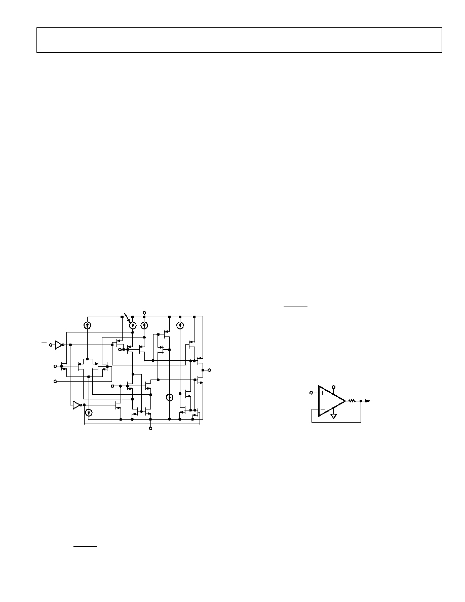
THEORY OF OPERATION
The AD859x amplifiers are CMOS, high output drive, rail-to-
rail input and output single-supply amplifiers designed for low
cost and high output current drive. The parts include a power
saving shutdown function that makes the AD8591/AD8592/
AD8594 op amps ideal for portable multimedia and
telecommunications applications.
Figure 33 shows the simplified schematic for the AD8591/AD8592/
AD8594 amplifiers. Two input differential pairs, consisting of
an n-channel pair (M1, M2) and a p-channel pair (M3, M4),
provide a rail-to-rail input common-mode range. The outputs of
the input differential pairs are combined in a compound folded-
cascode stage that drives the input to a second differential pair
gain stage. The outputs of the second gain stage provide the gate
voltage drive to the rail-to-rail output stage.
The rail-to-rail output stage consists of M15 and M16, which
are configured in a complementary common source configuration.
As with any rail-to-rail output amplifier, the gain of the output
stage, and thus the open-loop gain of the amplifier, is dependent
on the load resistance. In addition, the maximum output voltage
swing is directly proportional to the load current. The difference
between the maximum output voltage to the supply rails, known as
the dropout voltage, is determined by the on-channel resistance
of the AD8591/AD8592/AD8594 output transistors. The output
50A
100A
20A
VB2
M5
M8
M12
M15
M16
M11
OUT
M3
M4
M1
IN–
IN+
VB3
M6
M7
M10
20A
M13
50A
V+
V–
M9
M14
M2
*
M337
SD
INV
*
M340
*ALL CURRENT SOURCES GO TO 0A IN SHUTDOWN MODE.
INV
M31
M30
01106-
034
Figure 33. Simplified Schematic
INPUT VOLTAGE PROTECTION
Although not shown in the simplified schematic, ESD protection
diodes are connected from each input to each power supply rail.
These diodes are normally reverse-biased, but turn on if either
input voltage exceeds either supply rail by more than 0.6 V. If this
condition occurs, limit the input current to less than ±5 mA.
This is done by placing a resistor in series with the input(s).
The minimum resistor value should be
mA
5
, MAX
IN
V
R
≥
(1)
OUTPUT PHASE REVERSAL
The AD8591/AD8592/AD8594 are immune to output voltage
phase reversal with an input voltage within the supply voltages
of the device. However, if either of the inputs of the device exceeds
0.6 V outside of the supply rails, the output could exhibit phase
reversal. This is due to the ESD protection diodes becoming
forward-biased, thus causing the polarity of the input terminals
of the device to switch.
The technique recommended in the Input Voltage Protection
section should be applied in applications where the possibility
of input voltages exceeding the supply voltages exists.
OUTPUT SHORT-CIRCUIT PROTECTION
To achieve high output current drive and rail-to-rail performance,
the outputs of the AD859x family do not have internal short-
circuit protection circuitry. Although these amplifiers are
designed to sink or source as much as 250 mA of output current,
shorting the output directly to the positive supply could damage or
destroy the device. To protect the output stage, limit the maximum
output current to ±250 mA.
By placing a resistor in series with the output of the amplifier,
as shown in Figure 34, the output current can be limited. The
minimum value for RX is
mA
250
SY
X
V
R ≥
(2)
For a 5 V single-supply application, RX should be at least 20 Ω.
Because RX is inside the feedback loop, VOUT is not affected. The
trade-off in using RX is a slight reduction in output voltage
swing under heavy output current loads. RX also increases the
effective output impedance of the amplifier to RO + RX, where RO
is the output impedance of the device.
RX
20
VOUT
AD8592
+5V
VIN
01
10
6-
03
5
Figure 34. Output Short-Circuit Protection
POWER DISSIPATION
Although the AD859x amplifiers are able to provide load
currents of up to 250 mA, proper attention should be given to
not exceeding the maximum junction temperature for the device.
The junction temperature equation is
TJ
= PDISS × θJA + TA
(3)
where:
TJ
is the AD859x junction temperature.
PDISS
is the AD859x power dissipation.
θJA
is the AD859x junction-to-ambient thermal resistance of the
package.
TA
is the ambient temperature of the circuit.
相关PDF资料 |
PDF描述 |
|---|---|
| TSW-107-26-L-D | CONN HEADER 14POS .100" DL GOLD |
| MIC7300BM5 TR | IC OP AMP R-R IN/OUT SOT23-5 |
| TSW-108-26-L-D | CONN HEADER 16POS .100" DL GOLD |
| TSW-109-26-L-D | CONN HEADER 18POS .100" DL GOLD |
| MIC7122BMM TR | IC OP AMP DUAL R-R IN/OUT 8MSOP |
相关代理商/技术参数 |
参数描述 |
|---|---|
| AD8594ARZ-REEL | 功能描述:IC OPAMP GP R-R CMOS 3MHZ 16SOIC RoHS:是 类别:集成电路 (IC) >> Linear - Amplifiers - Instrumentation 系列:- 标准包装:2,500 系列:- 放大器类型:通用 电路数:1 输出类型:满摆幅 转换速率:0.11 V/µs 增益带宽积:350kHz -3db带宽:- 电流 - 输入偏压:4nA 电压 - 输入偏移:20µV 电流 - 电源:260µA 电流 - 输出 / 通道:20mA 电压 - 电源,单路/双路(±):2.7 V ~ 36 V,±1.35 V ~ 18 V 工作温度:-40°C ~ 85°C 安装类型:表面贴装 封装/外壳:8-SOIC(0.154",3.90mm 宽) 供应商设备封装:8-SO 包装:带卷 (TR) |
| AD8594ARZ-REEL7 | 制造商:Analog Devices 功能描述:OP Amp Quad GP R-R I/O 6V 16-Pin SOIC N T/R |
| AD8597 | 制造商:AD 制造商全称:Analog Devices 功能描述:30 V, Low Noise, Rail-to-Rail |
| AD8597_08 | 制造商:AD 制造商全称:Analog Devices 功能描述:Single and Dual, Ultralow Distortion, Ultralow Noise Op Amps |
| AD8597ACPZ-R2 | 功能描述:IC OPAMP SGL 1.1NV LN 8LFCSP RoHS:是 类别:集成电路 (IC) >> Linear - Amplifiers - Instrumentation 系列:- 标准包装:2,500 系列:- 放大器类型:通用 电路数:4 输出类型:- 转换速率:0.6 V/µs 增益带宽积:1MHz -3db带宽:- 电流 - 输入偏压:45nA 电压 - 输入偏移:2000µV 电流 - 电源:1.4mA 电流 - 输出 / 通道:40mA 电压 - 电源,单路/双路(±):3 V ~ 32 V,±1.5 V ~ 16 V 工作温度:0°C ~ 70°C 安装类型:表面贴装 封装/外壳:14-TSSOP(0.173",4.40mm 宽) 供应商设备封装:14-TSSOP 包装:带卷 (TR) 其它名称:LM324ADTBR2G-NDLM324ADTBR2GOSTR |
发布紧急采购,3分钟左右您将得到回复。