- 您现在的位置:买卖IC网 > PDF目录3537 > AD8597ARZ-REEL7 (Analog Devices Inc)IC OPAMP GP 10MHZ ULDIST 8SOIC PDF资料下载
参数资料
| 型号: | AD8597ARZ-REEL7 |
| 厂商: | Analog Devices Inc |
| 文件页数: | 7/20页 |
| 文件大小: | 0K |
| 描述: | IC OPAMP GP 10MHZ ULDIST 8SOIC |
| 设计资源: | Automated Calibration Technique That Reduces AD5360 Offset Voltage to Less Than 1 mV (CN0123) |
| 标准包装: | 1,000 |
| 放大器类型: | 通用 |
| 电路数: | 1 |
| 转换速率: | 16 V/µs |
| 增益带宽积: | 10MHz |
| 电流 - 输入偏压: | 25nA |
| 电压 - 输入偏移: | 10µV |
| 电流 - 电源: | 5mA |
| 电流 - 输出 / 通道: | 52mA |
| 电压 - 电源,单路/双路(±): | 9 V ~ 36 V,±4.5 V ~ 18 V |
| 工作温度: | -40°C ~ 125°C |
| 安装类型: | 表面贴装 |
| 封装/外壳: | 8-SOIC(0.154",3.90mm 宽) |
| 供应商设备封装: | 8-SO |
| 包装: | 带卷 (TR) |
Data Sheet
AD8597/AD8599
Rev. E | Page 15 of 20
FUNCTIONAL OPERATION
INPUT VOLTAGE RANGE
therefore, care is required to ensure that both inputs do not
exceed the input voltage range. Under normal negative feedback
operating conditions, the amplifier corrects its output to ensure
that the two inputs are at the same voltage. However, if either
input exceeds the input voltage range, the loop opens and large
currents begin to flow through the ESD protection diodes in the
amplifier.
These diodes are connected between the inputs and each supply
rail to protect the input transistors against an electrostatic discharge
event and they are normally reverse-biased. However, if the
input voltage exceeds the supply voltage, these ESD diodes can
become forward-biased. Without current limiting, excessive
amounts of current may flow through these diodes, causing
permanent damage to the device. If inputs are subject to over-
voltage, insert appropriate series resistors to limit the diode
current to less than 5 mA maximum.
The input stage has two diodes between the input pins to protect
the differential pair. Under high slew rate conditions, when the
op amp is connected as a voltage follower, the diodes may become
forward-biased and the source may try to drive the output.
Place a small resistor in the feedback loop and in the noninverting
input. The noise of a 100 Ω resistor at room temperature is
Thus, there is a tradeoff between noise performance and
protection. If possible, place limiting earlier in the signal path.
For further details, see the Amplifier Input Protection… Friend
or Foe? article at http://www.analog.com/amplifier_input.
Because of the large transistors used to achieve low noise, the
input capacitance may seem rather high. To take advantage of
the low noise performance, impedance around the op amp must
be low, less than 500 Ω. Under these conditions, the pole from
the input capacitance must be greater than 50 MHz, which does
not affect the signal bandwidth.
OUTPUT PHASE REVERSAL
Output phase reversal occurs in some amplifiers when the input
common-mode voltage range is exceeded. As the common-mode
voltage is moved outside the input voltage range, the outputs of
these amplifiers can suddenly jump in the opposite direction to
the supply rail. This is the result of the differential input pair
shutting down that causes a radical shifting of internal voltages
that results in the erratic output behavior.
The AD8597/AD8599 amplifiers are carefully designed to prevent
any output phase reversal if both inputs are maintained within
the specified input voltage range. If one or both inputs exceed
the input voltage range but remain within the supply rails, the
op amp specifications, such as CMRR, are not guaranteed, but
the output remains close to the correct value.
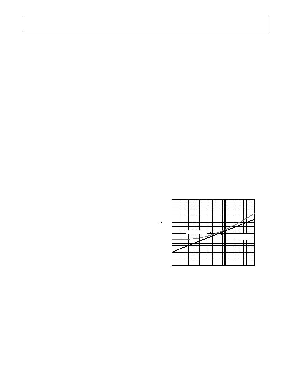
NOISE AND SOURCE IMPEDANCE CONSIDERATIONS
achieved with special input transistors running at high collector
current. Therefore, it is important to consider the total input-
referred noise (eN total), which includes contributions from
voltage noise (eN), current noise (iN), and resistor noise
(√4 kTRS).
eN total = [eN2 + 4 kTRS + (iN × RS)2]1/2
(1)
where RS is the total input source resistance.
Because optimum dc performance is obtained with matched
source resistances, this case is considered even though it is clear
from Equation 1 that eliminating the balancing source resistance
lowers the total noise by reducing the total RS by a factor of 2.
At a very low source resistance (RS < 50 Ω), the voltage noise of the
amplifier dominates. As source resistance increases, the Johnson
noise of RS dominates until a higher resistance of RS > 2 kΩ is
achieved; the current noise component is larger than the
resistor noise.
100
1
10
0.1
10
100
1k
10k
TOTA
L
N
OIS
E
(
nV
/
H
z
)
SOURCE RESISTANCE (Ω)
06274-
076
TOTAL NOISE
RESISTOR NOISE
ONLY
Figure 58. Noise vs. Source Resistance
相关PDF资料 |
PDF描述 |
|---|---|
| P6KE16AHE3/73 | TVS 600W 16V 5% UNIDIR AXIAL |
| GEC33SFBN-M30 | CONN HEADER 33PS .100 SINGLE SMD |
| P6KE160AHE3/73 | TVS 600W 160V 5% UNIDIR AXIAL |
| OP177FSZ-REEL7 | IC OPAMP GP PREC LN 8SOIC |
| PEC15DBDN | CONN HEADER .100 DUAL R/A 30POS |
相关代理商/技术参数 |
参数描述 |
|---|---|
| AD8598 | 制造商:AD 制造商全称:Analog Devices 功能描述:Dual 7 ns Single Supply Comparator |
| AD8598AN | 制造商:Analog Devices 功能描述:COMPARATOR DUAL IND SPEC 8598 DIP |
| AD8598AR | 制造商:AD 制造商全称:Analog Devices 功能描述:Dual 7 ns Single Supply Comparator |
| AD8598ARU | 制造商:Analog Devices 功能描述: |
| AD8598ARU-REEL | 制造商:Rochester Electronics LLC 功能描述:DUAL SUPPLY 5NS COMPARATO - Tape and Reel 制造商:Analog Devices 功能描述: |
发布紧急采购,3分钟左右您将得到回复。