参数资料
| 型号: | AD8604DRZ |
| 厂商: | Analog Devices Inc |
| 文件页数: | 8/24页 |
| 文件大小: | 0K |
| 描述: | IC OPAMP QUAD R-R I/O 14SOIC |
| 标准包装: | 56 |
| 放大器类型: | 通用 |
| 电路数: | 4 |
| 输出类型: | 满摆幅 |
| 转换速率: | 6 V/µs |
| 增益带宽积: | 8.4MHz |
| 电流 - 输入偏压: | 0.2pA |
| 电压 - 输入偏移: | 1300µV |
| 电流 - 电源: | 750µA |
| 电流 - 输出 / 通道: | 50mA |
| 电压 - 电源,单路/双路(±): | 2.7 V ~ 5.5 V |
| 工作温度: | -40°C ~ 125°C |
| 安装类型: | 表面贴装 |
| 封装/外壳: | 14-TSSOP(0.173",4.40mm 宽) |
| 供应商设备封装: | 14-TSSOP |
| 包装: | 管件 |
AD8601/AD8602/AD8604
Rev. G | Page 16 of 24
INPUT OVERVOLTAGE PROTECTION
As with any semiconductor device, if a condition could exist
that could cause the input voltage to exceed the power supply,
the device’s input overvoltage characteristic must be considered.
Excess input voltage energizes the internal PN junctions in the
AD860x, allowing current to flow from the input to the supplies.
This input current does not damage the amplifier, provided it is
limited to 5 mA or less. This can be ensured by placing a resistor in
series with the input. For example, if the input voltage could
exceed the supply by 5 V, the series resistor should be at least
(5 V/5 mA) = 1 kΩ. With the input voltage within the supply
rails, a minimal amount of current is drawn into the inputs,
which, in turn, causes a negligible voltage drop across the series
resistor. Therefore, adding the series resistor does not adversely
affect circuit performance.
OVERDRIVE RECOVERY
Overdrive recovery is defined as the time it takes the output of
an amplifier to come off the supply rail when recovering from
an overload signal. This is tested by placing the amplifier in a
closed-loop gain of 10 with an input square wave of 2 V p-p
while the amplifier is powered from either 5 V or 3 V.
The AD860x has excellent recovery time from overload conditions.
The output recovers from the positive supply rail within 200 ns
at all supply voltages. Recovery from the negative rail is within
500 ns at a 5 V supply, decreasing to within 350 ns when the
device is powered from 2.7 V.
POWER-ON TIME
The power-on time is important in portable applications where
the supply voltage to the amplifier may be toggled to shut down
the device to improve battery life. Fast power-up behavior ensures
that the output of the amplifier quickly settles to its final voltage,
improving the power-up speed of the entire system. When the
supply voltage reaches a minimum of 2.5 V, the AD860x settles to
a valid output within 1 μs. This turn-on response time is faster
than many other precision amplifiers, which can take tens or
hundreds of microseconds for their outputs to settle.
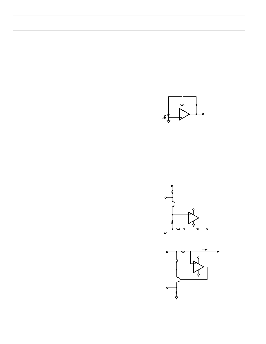
USING THE AD8602 IN HIGH SOURCE IMPEDANCE
APPLICATIONS
The CMOS rail-to-rail input structure of the AD860x allows
these amplifiers to have very low input bias currents, typically
0.2 pA. This allows the AD860x to be used in any application
that has a high source impedance or must use large value
resistances around the amplifier. For example, the photodiode
amplifier circuit shown in Figure 56 requires a low input bias
current op amp to reduce output voltage error. The AD8601
minimizes offset errors due to its low input bias current and low
offset voltage.
The current through the photodiode is proportional to the incident
light power on its surface. The 4.7 MΩ resistor converts this current
into a voltage, with the output of the AD8601 increasing at 4.7 V/μA.
The feedback capacitor reduces excess noise at higher frequencies
by limiting the bandwidth of the circuit to
()
F
C
π
BW
Ω
M
7
.
4
2
1
=
(1)
Using a 10 pF feedback capacitor limits the bandwidth to
approximately 3.3 kHz.
AD8601
10pF
(OPTIONAL)
VOUT
4.7V/A
4.7M
D1
01
52
5-
05
6
Figure 56. Amplifier Photodiode Circuit
HIGH SIDE AND LOW SIDE, PRECISION CURRENT
MONITORING
Because of its low input bias current and low offset voltage, the
AD860x can be used for precision current monitoring. The true
rail-to-rail input feature of the AD860x allows the amplifier to
monitor current on either the high side or the low side. Using both
amplifiers in an AD8602 provides a simple method for monitoring
both current supply and return paths for load or fault detection.
01
52
5-
0
5
7
1/2 AD8602
RETURN TO
GROUND
RSENSE
0.1
R1
100
R2
249k
Q1
2N3904
MONITOR
OUTPUT
3V
Figure 57. Low-Side Current Monitor
015
25
-05
8
3V
IL
V+
3V
MONITOR
OUTPUT
R1
100
R2
2.49k
RSENSE
0.1
Q1
2N3905
1/2 AD8602
Figure 58. High-Side Current Monitor
相关PDF资料 |
PDF描述 |
|---|---|
| MP2-P240-51M1-TG30 | CONN INV HEADER 2-FB 240POS 5ROW |
| 94747 | TERM RING INSUL 12-10AWG #1/2 |
| 5-534206-1 | CONN RECEPT 2POS .100 VERT DUAL |
| MMA23-0141R1 | CONN RACK/PANEL 14POS 5A |
| ADA4851-4YRUZ-RL7 | IC OPAMP VF R-R QUAD LP 14TSSOP |
相关代理商/技术参数 |
参数描述 |
|---|---|
| AD8604DRZ-REEL | 功能描述:IC OPAMP QUAD R-R I/O 14SOIC RoHS:是 类别:集成电路 (IC) >> Linear - Amplifiers - Instrumentation 系列:- 标准包装:160 系列:- 放大器类型:通用 电路数:4 输出类型:满摆幅 转换速率:10 V/µs 增益带宽积:9MHz -3db带宽:- 电流 - 输入偏压:1pA 电压 - 输入偏移:250µV 电流 - 电源:730µA 电流 - 输出 / 通道:28mA 电压 - 电源,单路/双路(±):2.7 V ~ 5.5 V,±1.35 V ~ 2.75 V 工作温度:-40°C ~ 125°C 安装类型:表面贴装 封装/外壳:16-SOIC(0.154",3.90mm 宽) 供应商设备封装:16-SOIC N 包装:管件 |
| AD8605 | 制造商:AD 制造商全称:Analog Devices 功能描述:精密、低噪声、CMOS轨到轨输入/输出运算放大器 |
| AD8605_08 | 制造商:AD 制造商全称:Analog Devices 功能描述:Precision, Low Noise, CMOS, Rail-to-Rail, Input/Output Operational Amplifiers |
| AD8605ACB | 制造商:未知厂家 制造商全称:未知厂家 功能描述:AD8605ACB: Precision Low Noise CMOS Rail-to-Rail Input/Output Operational Amplifiers Prelim Data Sheet (Rev. PrA. 10/02) |
| AD8605ACB-REEL | 制造商:Analog Devices 功能描述:OP Amp Single GP R-R I/O 5.5V 5-Pin WLCSP T/R 制造商:Analog Devices 功能描述:OP AMP SGL GP R-R I/O 5.5V 5PIN WLCSP - Tape and Reel |
发布紧急采购,3分钟左右您将得到回复。