- 您现在的位置:买卖IC网 > PDF目录5404 > AD8607ARMZ-R2 (Analog Devices Inc)IC OPAMP GP R-R CMOS DUAL 8MSOP PDF资料下载
参数资料
| 型号: | AD8607ARMZ-R2 |
| 厂商: | Analog Devices Inc |
| 文件页数: | 4/16页 |
| 文件大小: | 0K |
| 描述: | IC OPAMP GP R-R CMOS DUAL 8MSOP |
| 标准包装: | 1 |
| 放大器类型: | 通用 |
| 电路数: | 2 |
| 输出类型: | 满摆幅 |
| 转换速率: | 0.1 V/µs |
| 增益带宽积: | 400kHz |
| 电流 - 输入偏压: | 0.2pA |
| 电压 - 输入偏移: | 12µV |
| 电流 - 电源: | 40µA |
| 电流 - 输出 / 通道: | 70mA |
| 电压 - 电源,单路/双路(±): | 1.8 V ~ 5 V,±0.9 V ~ 2.5 V |
| 工作温度: | -40°C ~ 125°C |
| 安装类型: | 表面贴装 |
| 封装/外壳: | 8-TSSOP,8-MSOP(0.118",3.00mm 宽) |
| 供应商设备封装: | 8-MSOP |
| 包装: | 剪切带 (CT) |
| 其它名称: | AD8607ARMZ-R2CT |
AD8603/AD8607/AD8609
Rev. C | Page 12 of 16
APPLICATIONS
NO PHASE REVERSAL
The AD8603/AD8607/AD8609 do not exhibit phase inversion
even when the input voltage exceeds the maximum input
common-mode voltage. Phase reversal can cause permanent
damage to the amplifier, resulting in system lockups. The
AD8603/AD8607/AD8609 can handle voltages of up to 1 V
over the supply.
V
O
LT
A
G
E
(
1V/
D
IV)
TIME (4s/DIV)
VS = ±2.5V
VIN = 6V p-p
AV = 1
RL = 10k
VIN
VOUT
04
35
6-
0
41
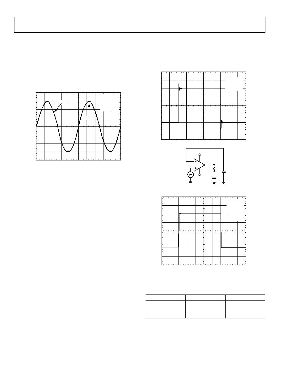
Figure 41. No Phase Response
INPUT OVERVOLTAGE PROTECTION
If a voltage 1 V higher than the supplies is applied at either
input, the use of a limiting series resistor is recommended. If
both inputs are used, each one should be protected with a
series resistor.
To ensure good protection, the current should be limited to a
maximum of 5 mA. The value of the limiting resistor can be
determined from the following equation:
(VIN VS)/(RS + 200 Ω) ≤ 5 mA
DRIVING CAPACITIVE LOADS
The AD8603/AD8607/AD8609 are capable of driving large
capacitive loads without oscillating. Figure 42 shows the output
of the AD8603/AD8607/AD8609 in response to a 100 mV input
signal, with a 2 nF capacitive load.
Although it is configured in positive unity gain (the worst case),
the AD8603 shows less than 20% overshoot. Simple additional
circuitry can eliminate ringing and overshoot.
One technique is the snubber network, which consists of a
series RC and a resistive load (see Figure 43). With the snubber
in place, the AD8603/AD8607/AD8609 are capable of driving
capacitive loads of 2 nF with no ringing and less than 3%
overshoot.
The use of the snubber circuit is usually recommended for unity
gain configurations. Higher gain configurations help improve
the stability of the circuit. Figure 44 shows the same output
response with the snubber in place.
VS = ±0.9V
VIN = 100mV
CL = 2nF
RL = 10k
0
43
56
-04
2
Figure 42. Output Response to a 2 nF Capacitive Load, Without Snubber
04
35
6-
04
3
CS
47pF
VCC
VEE
RS
150
200mV
CL
V+
V–
–
+
Figure 43. Snubber Network
VSY = ±0.9V
VIN = 100mV
CL = 2nF
RL = 10k
RS = 150
CS = 470pF
0
435
6-
0
44
Figure 44. Output Response to a 2 nF Capacitive Load with Snubber
Optimum values for RS and CS are determined empirically;
Table 5 lists a few starting values.
Table 5. Optimum Values for the Snubber Network
CL (pF)
RS (Ω)
CS (pF)
100 to ~500
500
680
1500
100
330
1600 to ~2000
400
100
相关PDF资料 |
PDF描述 |
|---|---|
| 1-322337-1 | CONN TERM RING 16-14AWG #10 |
| LT1037CSW#TR | IC OPAMP PREC SGL HI SPD 16SOIC |
| AD8672ARMZ-R2 | IC OPAMP GP 10MHZ DUAL LN 8MSOP |
| 3404.0116.24 | FUSE 2A 125V SMD SLOW |
| 3404.0115.24 | FUSE 1.5A 125V SMD SLOW |
相关代理商/技术参数 |
参数描述 |
|---|---|
| AD8607ARMZ-R21 | 制造商:AD 制造商全称:Analog Devices 功能描述:Precision Micropower, Low Noise CMOS, Rail-to-Rail Input/Output Operational Amplifiers |
| AD8607ARMZ-REEL | 功能描述:IC OPAMP GP R-R CMOS DUAL 8MSOP RoHS:是 类别:集成电路 (IC) >> Linear - Amplifiers - Instrumentation 系列:- 产品培训模块:Differential Circuit Design Techniques for Communication Applications 标准包装:1 系列:- 放大器类型:RF/IF 差分 电路数:1 输出类型:差分 转换速率:9800 V/µs 增益带宽积:- -3db带宽:2.9GHz 电流 - 输入偏压:3µA 电压 - 输入偏移:- 电流 - 电源:40mA 电流 - 输出 / 通道:- 电压 - 电源,单路/双路(±):3 V ~ 3.6 V 工作温度:-40°C ~ 85°C 安装类型:表面贴装 封装/外壳:16-VQFN 裸露焊盘,CSP 供应商设备封装:16-LFCSP-VQ 包装:剪切带 (CT) 产品目录页面:551 (CN2011-ZH PDF) 其它名称:ADL5561ACPZ-R7CT |
| AD8607ARMZ-REEL1 | 制造商:AD 制造商全称:Analog Devices 功能描述:Precision Micropower, Low Noise CMOS, Rail-to-Rail Input/Output Operational Amplifiers |
| AD8607AR-REEL | 制造商:Analog Devices 功能描述:OP Amp Dual GP R-R I/O 制造商:Analog Devices 功能描述:OP Amp Dual GP R-R I/O ±2.5V/5V 8-Pin SOIC N T/R |
| AD8607AR-REEL7 | 制造商:Analog Devices 功能描述:OP Amp Dual GP R-R I/O 制造商:Rochester Electronics LLC 功能描述:DUAL, PRECISION CMOS RAIL-RAIL OP AMP - Tape and Reel |
发布紧急采购,3分钟左右您将得到回复。