- 您现在的位置:买卖IC网 > PDF目录10791 > AD8612ARUZ (Analog Devices Inc)IC COMP DUAL 4NS FAST 14-TSSOP PDF资料下载
参数资料
| 型号: | AD8612ARUZ |
| 厂商: | Analog Devices Inc |
| 文件页数: | 3/20页 |
| 文件大小: | 0K |
| 描述: | IC COMP DUAL 4NS FAST 14-TSSOP |
| 标准包装: | 96 |
| 类型: | 带锁销 |
| 元件数: | 2 |
| 输出类型: | 补充型,TTL |
| 电压 - 电源,单路/双路(±): | 3 V ~ 5 V |
| 电压 - 输入偏移(最小值): | 7mV @ 5V |
| 电流 - 输入偏压(最小值): | 6µA @ 5V |
| 电流 - 静态(最大值): | 10mA,4mA |
| CMRR, PSRR(标准): | 85dB CMRR,73dB PSRR |
| 传输延迟(最大): | 5.5ns |
| 工作温度: | -40°C ~ 85°C |
| 封装/外壳: | 14-TSSOP(0.173",4.40mm 宽) |
| 安装类型: | 表面贴装 |
| 包装: | 管件 |
| 产品目录页面: | 764 (CN2011-ZH PDF) |
AD8611/AD8612
Rev. A | Page 11 of 20
OUTPUT LOADING CONSIDERATIONS
The AD8611 can deliver up to 10 mA of output current without
increasing its propagation delay. The outputs of the device
should not be connected to more than 40 TTL input logic gates
or drive less than 400 Ω of load resistance.
The AD8611 output has a typical output swing between ground
and 1 V below the positive supply voltage. Decreasing the
output load resistance to ground lowers the maximum output
voltage due to the increase in output current. Table 6 shows the
typical output high voltage vs. load resistance to ground.
Table 6. Maximum Output Voltage vs. Resistive Load
Output Load to Ground
V+ VOUT, HI (typ)
300 Ω
1.5 V
500 Ω
1.3 V
1 kΩ
1.2 V
10 kΩ
1.1 V
>20 kΩ
1.0 V
Connecting a 500 Ω to 2 kΩ pull-up resistor to V+ on the
output helps increase the output voltage so that it is closer to the
positive rail; in this configuration, however, the output voltage
will not reach its maximum until 20 ns to 50 ns after the output
voltage switches. This is due to the R-C time constant between
the pull-up resistor and the output and load capacitances. The
output pull-up resistor cannot improve propagation delay.
The AD8611 is stable with all values of capacitive load; however,
loading an output with greater than 30 pF increases the
propagation delay of that channel. Capacitive loads greater than
500 pF also create some ringing on the output wave. Table 7
shows propagation delay vs. several values of load capacitance.
The loading on one output of the AD8611 does not affect the
propagation delay of the other output.
Table 7. Propagation Delay vs. Capacitive Load
CL (pF)
tPD Rising (ns)
tPD Falling (ns)
<10
3.5
33
5
100
8
7
390
14.5
10
680
26
15
USING THE LATCH
TO MAINTAIN A CONSTANT OUTPUT
With the VCC supply at a nominal 5 V, the latch input to the
AD8611/AD8612 can be used to retain data at the output of the
comparator. When the latch voltage goes high, the output
voltage remains in its previous state, independent of changes in
the input voltage.
The setup time for the AD8611/AD8612 is 0.5 ns and the hold
time is 0.5 ns. Setup time is defined as the minimum amount of
time the input voltage must remain in a valid state before the
latch is activated for the latch to function properly. Hold time is
defined as the amount of time the input must remain constant
after the latch voltage goes high for the output to remain latched
to its voltage.
The latch input is TTL and CMOS compatible, so a logic high is
a minimum of 2.0 V and a logic low is a maximum of 0.8 V. The
latch circuitry in the AD8611/AD8612 has no built-in
hysteresis. At or below approximately 4.1 V, the latch pin
becomes unresponsive and should normally be tied low for low
VCC operation.
INPUT STAGE AND BIAS CURRENTS
The AD8611 and AD8612 each use a bipolar PNP differential
input stage. This enables the input common-mode voltage range
to extend from within 2.0 V of the positive supply voltage to
200 mV below the negative supply voltage. Therefore, using a
single 5 V supply, the input common-mode voltage range is
200 mV to +3.0 V. Input common-mode voltage is the average
of the voltages at the two inputs. For proper operation, the input
common-mode voltage should be kept within the common-
mode voltage range.
The input bias current for the AD8611/AD8612 is 4 μA, which
is the amount of current that flows from each input of the
comparator. This bias current goes to zero on an input that is
high and doubles on an input that is low, which is a characteristic
common to any bipolar comparator. Care should be taken in
choosing resistances to be connected around the comparator
because large resistors could significantly decrease the voltage
due to the input bias current.
The input capacitance for the AD8611/AD8612 is typically 3 pF.
This is measured by inserting a 5 kΩ source resistance in series
with the input and measuring the change in propagation delay.
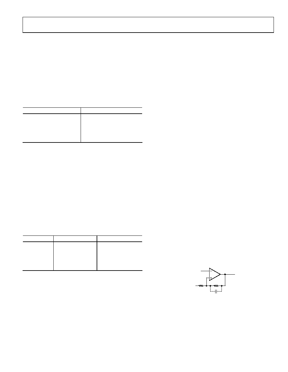
USING HYSTERESIS
Hysteresis can easily be added to a comparator through the
addition of positive feedback. Adding hysteresis to a comparator
offers an advantage in noisy environments where it is undesirable
for the output to toggle between states when the input signal is
close to the switching threshold. Figure 24 shows a simple method
for configuring the AD8611 or AD8612 with hysteresis.
VREF
R1
SIGNAL
COMPARATOR
R2
CF
0
6
010
-02
1
Figure 24. Configuring the AD8611/AD8612 with Hysteresis
In Figure 24, the input signal is connected directly to the
inverting input of the comparator. The output is fed back to the
noninverting input through R1 and R2. The ratio of R1 to
R1 + R2 establishes the width of the hysteresis window, with
VREF setting the center of the window, or the average switching
voltage. The QA or QB output switches low when the input
相关PDF资料 |
PDF描述 |
|---|---|
| VI-244-IW-S | CONVERTER MOD DC/DC 48V 100W |
| AD5301BRTZ-REEL | IC DAC 8BIT 2WIRE I2C SOT23-6 |
| B37981M1682K054 | CAP CER 6800PF 100V 10% RADIAL |
| AD8522AR-REEL | IC DAC DUAL 12BIT 5V 14-SOIC |
| LTC1445IDHD#PBF | IC COMP QD LP 1.221VREF 16-DFN |
相关代理商/技术参数 |
参数描述 |
|---|---|
| AD8612ARUZ | 制造商:Analog Devices 功能描述:IC DUAL COMPARATOR |
| AD8612ARUZ-REEL | 功能描述:IC COMP DUAL 4NS FAST 14-TSSOP RoHS:是 类别:集成电路 (IC) >> 线性 - 比较器 系列:- 产品培训模块:Lead (SnPb) Finish for COTS Obsolescence Mitigation Program 标准包装:2,500 系列:- 类型:通用 元件数:1 输出类型:CMOS,推挽式,满摆幅,TTL 电压 - 电源,单路/双路(±):2.5 V ~ 5.5 V,±1.25 V ~ 2.75 V 电压 - 输入偏移(最小值):5mV @ 5.5V 电流 - 输入偏压(最小值):1pA @ 5.5V 电流 - 输出(标准):- 电流 - 静态(最大值):24µA CMRR, PSRR(标准):80dB CMRR,80dB PSRR 传输延迟(最大):450ns 磁滞:±3mV 工作温度:-40°C ~ 85°C 封装/外壳:6-WFBGA,CSPBGA 安装类型:表面贴装 包装:管件 其它名称:Q3554586 |
| AD8613 | 制造商:AD 制造商全称:Analog Devices 功能描述:Low Cost Micropower, Low Noise CMOS Rail-to- Rail, Input/Output Operational Amplifiers |
| AD8613_10 | 制造商:AD 制造商全称:Analog Devices 功能描述:Low Cost Micropower, Low Noise CMOS Rail-to-Rail, Input/Output Operational Amplifiers |
| AD8613AKSZ | 制造商:Analog Devices 功能描述:OP AMP RAIL-RAIL I/O SMD SC70-5 制造商:Analog Devices 功能描述:OP AMP, RAIL-RAIL I/O, SMD, SC70-5 |
发布紧急采购,3分钟左右您将得到回复。