- 您现在的位置:买卖IC网 > PDF目录5391 > AD8614ART-REEL7 (Analog Devices Inc)IC OPAMP GP R-R 5.5MHZ SOT23-5 PDF资料下载
参数资料
| 型号: | AD8614ART-REEL7 |
| 厂商: | Analog Devices Inc |
| 文件页数: | 2/16页 |
| 文件大小: | 0K |
| 描述: | IC OPAMP GP R-R 5.5MHZ SOT23-5 |
| 标准包装: | 1 |
| 放大器类型: | 通用 |
| 电路数: | 1 |
| 输出类型: | 满摆幅 |
| 转换速率: | 7.5 V/µs |
| 增益带宽积: | 5.5MHz |
| 电流 - 输入偏压: | 80nA |
| 电压 - 输入偏移: | 1000µV |
| 电流 - 电源: | 800µA |
| 电流 - 输出 / 通道: | 70mA |
| 电压 - 电源,单路/双路(±): | 5 V ~ 18 V |
| 工作温度: | -20°C ~ 85°C |
| 安装类型: | 表面贴装 |
| 封装/外壳: | SC-74A,SOT-753 |
| 供应商设备封装: | SOT-23-5 |
| 包装: | 剪切带 (CT) |
| 其它名称: | AD8614ART-REEL7CT |
AD8614/AD8644
Rev. B | Page 10 of 16
INPUT OVERVOLTAGE PROTECTION
As with any semiconductor device, whenever the condition
exists for the input to exceed either supply voltage, attention
needs to be paid to the input overvoltage characteristic. As an
overvoltage occurs, the amplifier can be damaged, depending
on the voltage level and the magnitude of the fault current.
When the input voltage exceeds either supply by more than
0.6 V, internal pin junctions energize, allowing current to flow
from the input to the supplies. Observing Figure 26, the
AD8614/AD8644 have 1.5 kΩ resistors in series with each
input, which helps to limit the current. This input current is not
inherently damaging to the device as long as it is limited to
5 mA or less. If the voltage is large enough to cause more than
5 mA of current to flow, an external series resistor should be
added. The size of this resistor is calculated by dividing the
maximum overvoltage by 5 mA and subtracting the internal
1.5 kΩ resistor. For example, if the input voltage could reach 100 V,
the external resistor should be (100 V ÷ 5 mA) – 1.5 kΩ = 18.5 kΩ.
This resistance should be placed in series with either or both
inputs if they are subjected to the overvoltages.
OUTPUT PHASE REVERSAL
The AD8614/AD8644 are immune to phase reversal as long as
the input voltage is limited to within the supply rails. Although
the device’s output does not change phase, large currents due to
input overvoltage can result, damaging the device. In applica-
tions where the possibility of an input voltage exceeding the
supply voltage exists, overvoltage protection should be used, as
described in the previous section.
POWER DISSIPATION
The maximum power that can be safely dissipated by the
AD8614/AD8644 is limited by the associated rise in junction
temperature. The maximum safe junction temperature is 150°C,
and should not be exceeded or device performance could suffer.
If this maximum is momentarily exceeded, proper circuit
operation is restored as soon as the die temperature is reduced.
Leaving the device in an overheated condition for an extended
period can result in permanent damage to the device.
To calculate the internal junction temperature of the
AD8614/AD8644, the following formula can be used:
TJ = PDISS × θJA + TA
where:
TJ is the AD8614/AD8644 junction temperature.
PDISS is the AD8614/AD8644 power dissipation.
θJA is the AD8614/AD8644 junction-to-ambient package thermal
resistance.
TA is the ambient temperature of the circuit.
The power dissipated by the device can be calculated as:
PDISS = ILOAD × (VS – VOUT)
where:
ILOAD is the AD8614/AD8644 output load current.
VS is the AD8614/AD8644 supply voltage.
VOUT is the AD8614/AD8644 output voltage.
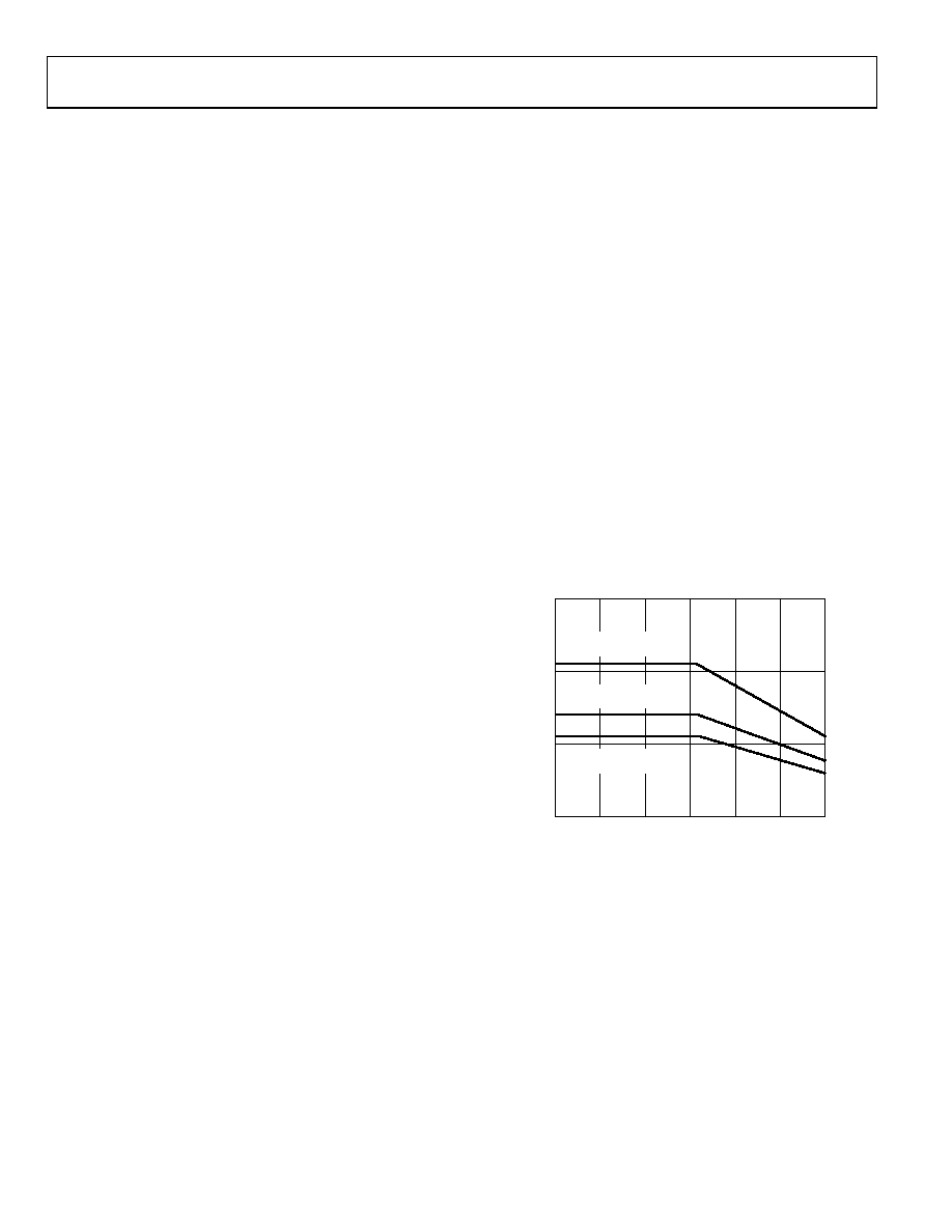
Figure 27 provides a convenient way to determine if the device
is being overheated. The maximum safe power dissipation can
be found graphically, based on the package type and the ambient
temperature around the package. By using the previous equation, it
is a simple matter to see if PDISS exceeds the device’s power derating
curve. To ensure proper operation, it is important to observe the
recommended derating curves shown in Figure 27.
1.5
0
1.0
0.5
MA
X
IMU
M
PO
W
E
R
D
ISS
IP
A
T
IO
N
(
W
)
AMBIENT TEMPERATURE (°C)
–35
–15
5
254565
85
14-LEAD SOIC PACKAGE
θJA = 120°C/W
14-LEAD TSSOP PACKAGE
θJA = 180°C/W
5-LEAD SOT-23 PACKAGE
θJA = 230°C/W
06
48
5-
0
27
Figure 27. Maximum Power Dissipation vs. Temperature
(5-Lead and 14-Lead Package Types)
UNUSED AMPLIFIERS
It is recommended that any unused amplifiers in the quad
package be configured as a unity-gain follower with a 1 kΩ
feedback resistor connected from the inverting input to the
output, and the noninverting input tied to the ground plane.
相关PDF资料 |
PDF描述 |
|---|---|
| LT6211IMS#TRPBF | IC AMP CURR FDBK DUAL R-R 10MSOP |
| OP27GSZ-REEL | IC OPAMP GP 8MHZ LN PREC 8SOIC |
| LT1782CS6#TRM | IC OPAMP R-R I/O MICRPWR SOT23-6 |
| MMK25-0091HU | CONN RACK/PANEL 9POS 5A |
| LT1783CS6#TRM | IC OPAMP R-R I/O MICRPWR SOT23-6 |
相关代理商/技术参数 |
参数描述 |
|---|---|
| AD8614ARTZ-REEL | 功能描述:IC OPAMP GP R-R 5.5MHZ SOT23-5 RoHS:是 类别:集成电路 (IC) >> Linear - Amplifiers - Instrumentation 系列:- 标准包装:2,500 系列:- 放大器类型:通用 电路数:1 输出类型:满摆幅 转换速率:0.11 V/µs 增益带宽积:350kHz -3db带宽:- 电流 - 输入偏压:4nA 电压 - 输入偏移:20µV 电流 - 电源:260µA 电流 - 输出 / 通道:20mA 电压 - 电源,单路/双路(±):2.7 V ~ 36 V,±1.35 V ~ 18 V 工作温度:-40°C ~ 85°C 安装类型:表面贴装 封装/外壳:8-SOIC(0.154",3.90mm 宽) 供应商设备封装:8-SO 包装:带卷 (TR) |
| AD8614ARTZ-REEL7 | 功能描述:IC OPAMP GP R-R 5.5MHZ SOT23-5 RoHS:是 类别:集成电路 (IC) >> Linear - Amplifiers - Instrumentation 系列:- 产品培训模块:Differential Circuit Design Techniques for Communication Applications 标准包装:1 系列:- 放大器类型:RF/IF 差分 电路数:1 输出类型:差分 转换速率:9800 V/µs 增益带宽积:- -3db带宽:2.9GHz 电流 - 输入偏压:3µA 电压 - 输入偏移:- 电流 - 电源:40mA 电流 - 输出 / 通道:- 电压 - 电源,单路/双路(±):3 V ~ 3.6 V 工作温度:-40°C ~ 85°C 安装类型:表面贴装 封装/外壳:16-VQFN 裸露焊盘,CSP 供应商设备封装:16-LFCSP-VQ 包装:剪切带 (CT) 产品目录页面:551 (CN2011-ZH PDF) 其它名称:ADL5561ACPZ-R7CT |
| AD8615 | 制造商:AD 制造商全称:Analog Devices 功能描述:Precision, 20 MHz, CMOS, Rail-to-Rail Input/Output Operational Amplifiers |
| AD8615_05 | 制造商:AD 制造商全称:Analog Devices 功能描述:Precision, 20 MHz, CMOS, Rail-to-Rail Input/Output Operational Amplifiers |
| AD8615_08 | 制造商:AD 制造商全称:Analog Devices 功能描述:Precision, 20 MHz, CMOS, Rail-to-Rail Input/Output Operational Amplifiers |
发布紧急采购,3分钟左右您将得到回复。