- 您现在的位置:买卖IC网 > PDF目录6093 > AD8616ARMZ-REEL (Analog Devices Inc)IC OPAMP GP R-R CMOS 24MHZ 8MSOP PDF资料下载
参数资料
| 型号: | AD8616ARMZ-REEL |
| 厂商: | Analog Devices Inc |
| 文件页数: | 4/20页 |
| 文件大小: | 0K |
| 描述: | IC OPAMP GP R-R CMOS 24MHZ 8MSOP |
| 标准包装: | 1 |
| 系列: | DigiTrim® |
| 放大器类型: | 通用 |
| 电路数: | 2 |
| 输出类型: | 满摆幅 |
| 转换速率: | 12 V/µs |
| 增益带宽积: | 24MHz |
| 电流 - 输入偏压: | 0.2pA |
| 电压 - 输入偏移: | 23µV |
| 电流 - 电源: | 1.7mA |
| 电流 - 输出 / 通道: | 150mA |
| 电压 - 电源,单路/双路(±): | 2.7 V ~ 5.5 V,±1.35 V ~ 2.75 V |
| 工作温度: | -40°C ~ 125°C |
| 安装类型: | 表面贴装 |
| 封装/外壳: | 8-TSSOP,8-MSOP(0.118",3.00mm 宽) |
| 供应商设备封装: | 8-MSOP |
| 包装: | 标准包装 |
| 产品目录页面: | 767 (CN2011-ZH PDF) |
| 其它名称: | AD8616ARMZ-REELDKR |
AD8615/AD8616/AD8618
Data Sheet
Rev. F | Page 12 of 20
OVERLOAD RECOVERY TIME
Overload recovery time is the time it takes the output of the
amplifier to come out of saturation and recover to its linear region.
Overload recovery is particularly important in applications where
small signals must be amplified in the presence of large transients.
Figure 40 and Figure 41 show the positive and negative overload
recovery times of the AD8616. In both cases, the time elapsed
before the AD8616 comes out of saturation is less than 1 μs. In
addition, the symmetry between the positive and negative recovery
times allows excellent signal rectification without distortion to the
output signal.
TIME (1s/DIV)
VS = ±2.5V
RL = 10k
AV = 100
VIN = 50mV
–50mV
+2.5V
0V
0
46
48
-04
0
Figure 40. Positive Overload Recovery
TIME (1s/DIV)
VS =±2.5V
RL = 10k
AV = 100
VIN = 50mV
+50mV
–
2.5V
0V
04
64
8-
04
1
Figure 41. Negative Overload Recovery
D/A CONVERSION
The AD8616 can be used at the output of high resolution DACs.
The low offset voltage, fast slew rate, and fast settling time make
the part suitable to buffer voltage output or current output
DACs.
Figure 42 shows an example of the AD8616 at the output of the
AD5542. The AD8616’s rail-to-rail output and low distortion
help maintain the accuracy needed in data acquisition systems
and automated test equipment.
AD5542
VOUT
UNIPOLAR
OUTPUT
AGND
DGND
REFS
1/2
AD8616
REFF
VDD
SERIAL
INTERFACE
0.1
F
0.1F
10F
5V
2.5V
+
CS
DIN
SCLK
LDAC
0
46
48
-0
42
Figure 42. Buffering DAC Output
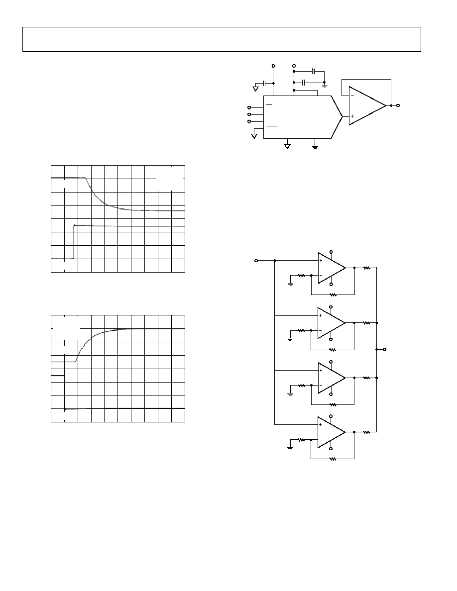
LOW NOISE APPLICATIONS
Although the AD8618 typically has less than 8 nV/√Hz of voltage
noise density at 1 kHz, it is possible to reduce it further. A simple
method is to connect the amplifiers in parallel, as shown in
Figure 43. The total noise at the output is divided by the square
root of the number of amplifiers. In this case, the total noise is
approximately 4 nV/√Hz at room temperature. The 100 Ω
resistor limits the current and provides an effective output
resistance of 50 Ω.
V–
R3
100
R1
10
V+
VIN
3
2
1
R2
1k
V–
R6
100
R4
10
V+
3
2
1
R5
1k
V–
R9
100
R7
10
V+
3
2
1
R8
1k
V–
R12
100
R10
10
V+
3
2
1
R11
1k
VOUT
04
64
8-
04
3
Figure 43. Noise Reduction
相关PDF资料 |
PDF描述 |
|---|---|
| 68602-226HLF | CONN HEADER 26POS .100 STR 15AU |
| 68602-132HLF | CONN HEADER 32POS .100 STR 30AU |
| AD8617ACPZ-R2 | IC OPAMP GP R-R CMOS LN 8LFCSP |
| 76382-408LF | CONN HEADER 8POS .100" R/A TIN |
| 10075025-G01-10ULF | CONN HEADER 10PS DL STR 2MM GOLD |
相关代理商/技术参数 |
参数描述 |
|---|---|
| AD8616ARMZ-REEL1 | 制造商:AD 制造商全称:Analog Devices 功能描述:Precision, 20 MHz, CMOS, Rail-to-Rail Input/Output Operational Amplifiers |
| AD8616AR-REEL | 制造商:Analog Devices 功能描述:OP Amp Dual GP R-R I/O 5V 8-Pin SOIC N T/R |
| AD8616AR-REEL7 | 制造商:Analog Devices 功能描述:OP Amp Dual GP R-R I/O 5V 8-Pin SOIC N T/R |
| AD8616ARZ | 功能描述:IC OPAMP GP R-R CMOS 24MHZ 8SOIC RoHS:是 类别:集成电路 (IC) >> Linear - Amplifiers - Instrumentation 系列:DigiTrim® 产品培训模块:Differential Circuit Design Techniques for Communication Applications 标准包装:1 系列:- 放大器类型:RF/IF 差分 电路数:1 输出类型:差分 转换速率:9800 V/µs 增益带宽积:- -3db带宽:2.9GHz 电流 - 输入偏压:3µA 电压 - 输入偏移:- 电流 - 电源:40mA 电流 - 输出 / 通道:- 电压 - 电源,单路/双路(±):3 V ~ 3.6 V 工作温度:-40°C ~ 85°C 安装类型:表面贴装 封装/外壳:16-VQFN 裸露焊盘,CSP 供应商设备封装:16-LFCSP-VQ 包装:剪切带 (CT) 产品目录页面:551 (CN2011-ZH PDF) 其它名称:ADL5561ACPZ-R7CT |
| AD8616ARZ | 制造商:Analog Devices 功能描述:OP AMP DUAL PRECISION RRI/O 8616 |
发布紧急采购,3分钟左右您将得到回复。